Method for controlling high-speed PCB signal impedance

A high-speed, signal technology, applied in the field of control, can solve the problems of signal reflection and distortion, achieve the effect of reasonable wiring and avoid signal reflection and distortion

Inactive Publication Date: 2015-03-25
SHENZHEN YIHUA COMP +2
View PDF4 Cites 14 Cited by
  • Summary
  • Abstract
  • Description
  • Claims
  • Application Information

AI Technical Summary

Problems solved by technology

[0004] In order to overcome the above technical problems, the present invention provides a method for controlling the impedance of high-speed PCB signals, which can ensure that high-speed PCB signals pass the impedance matching test at one time, and can avoid the occurrence of impedance mutations caused by high-speed PCB high-speed signal line testing. Signal integrity issues such as signal reflections and distortion

Method used


Image

  • Method for controlling high-speed PCB signal impedance

Examples


Embodiment Construction

[0020] The present invention will be further described below in conjunction with the accompanying drawings and embodiments.

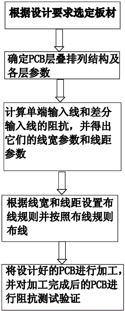
[0021] Such as figure 1 As shown, a method of controlling high-speed PCB signal impedance of the present invention includes

[0022] Next steps:

[0023] In the first step, the PCB material is selected according to impedance design requirements, preferably the PCB material is FR4 material.

[0024] The second step is to determine the PCB stacked arrangement structure and the parameters of each layer. The parameters include the dielectric constant and layer thickness of the board, and the dielectric constant is preferably 3.85GHZ.

[0025] The PCB stacked arrangement structure of the embodiment of the present invention is 8 layers, and the arrangement of the layers is that the ART01 layer is the TOP01 layer, the ART02 layer is the GND02 layer, the ART03 is the SIG03 layer, the ART04 layer is the POWER04 layer, the ART05 layer is the POWER05 layer, and ...


PUM

PropertyMeasurementUnit
Dielectric constantaaaaaaaaaa

Abstract

The invention provides a method for controlling high-speed PCB signal impedance. The method comprises the following steps that firstly, materials of PCBs are selected according to the design requirement; secondly, the PCB stacking and arranging structure and parameters of all layers are determined; thirdly, the impedance of a single-end input line and the impedance of a difference input line are calculated, and the line width parameter and the line distance parameter of the single-end input line and the difference input line are obtained; fourthly, a wiring rule is set according to the line width and the line distance, and wiring is carried out according to the wiring rule; finally, the designed PCBs are machined, and impedance testing and verifying are carried out on the machined PCBs. According to the method, based on the stacking structure of the reasonable design of eight layers of PCBs, a high-speed PCB signal can pass the impedance matching test at a time through the impedance matching and the reasonable wiring, and the problems of signal reflection and distortion and other signal integrity problems caused by sudden impedance change in a high-speed PCB signal line test can be avoided.

Description

technical field [0001] The invention relates to a control method, in particular to a method for controlling high-speed PCB signal impedance. Background technique [0002] With the increase of integrated circuit switching speed and the increase of PCB (Printed Circuit Board) board density, the high frequency and narrow edge of signals in high-speed PCB design make the signal integrity (Signal Integrity (SI)) problem become unnegligible , but also extremely challenging. In high-speed PCB design, if the design problem of signal integrity cannot be well solved, it may cause a fatal error in high-speed PCB design, which will greatly reduce the quality of signal transmission on the PCB, waste financial and material resources, prolong the development cycle, and reduce the design cost. efficiency. We know that the quality of signal transmission on PCB directly affects the performance of PCB, which is related to the requirements of PCB impedance design. In high-speed PCB design, t...

Claims


Application Information

Patent Timeline
IPC IPC(8): H05K3/46
CPCH05K3/46H05K3/0005H05K2203/30
Inventor 杨鹏
Owner SHENZHEN YIHUA COMP
Why Eureka
Try Eureka