Packaging structure and preparation method of OLED (organic light emitting diode) panel

A packaging structure and panel technology, which is applied in semiconductor/solid-state device manufacturing, electrical components, transistors, etc., can solve problems such as poor splits, achieve neat sections, obvious buffering effects, and avoid uneven splits

Inactive Publication Date: 2015-04-01
EVERDISPLAY OPTRONICS (SHANGHAI) CO LTD
View PDF4 Cites 24 Cited by
  • Summary
  • Abstract
  • Description
  • Claims
  • Application Information

AI Technical Summary

Problems solved by technology

[0004] In view of the above-mentioned problems in the prior art that are prone to poor splitting when the panel is cut, the present invention provides a method for preparing an OLED panel, including:

Method used


Image

  • Packaging structure and preparation method of OLED (organic light emitting diode) panel
  • Packaging structure and preparation method of OLED (organic light emitting diode) panel
  • Packaging structure and preparation method of OLED (organic light emitting diode) panel

Examples


Embodiment Construction

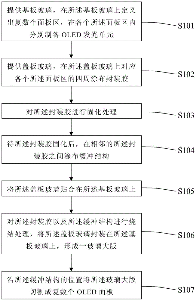
[0038] In order to make the object, technical solution and advantages of the present invention clearer, the present invention will be further described in detail below in conjunction with the accompanying drawings and embodiments. It should be understood that the specific embodiments described here are only used to explain the present invention, not to limit the present invention.

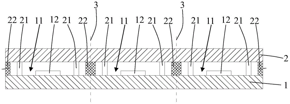
[0039] The packaging structure of the OLED panel of the present invention includes:

[0040] A substrate glass and a cover glass encapsulated in the substrate glass;

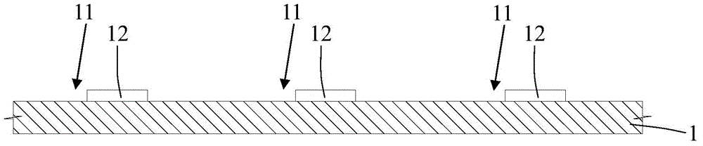
[0041] A panel area is defined on the substrate glass, and an OLED light-emitting unit is prepared in the panel area;

[0042] An encapsulant is provided between the substrate glass and the cover glass, the encapsulant is arranged around the panel area, and a buffer structure is provided on the outside of the encapsulant, one side of the buffer structure is in contact with the Align the sides of the substrate glass. Preferably, gl...


PUM


Abstract

The invention discloses a packaging structure and a preparation method of an OLED (organic light emitting diode) panel. The preparation method comprises the following steps of providing substrate glass, defining a plurality of panel areas on the substrate glass, and respectively preparing an OLED light emitting unit in each panel area; providing cover plate glass, and coating packaging glue around the parts, corresponding to each panel area, of the cover plate glass; curing the packaging glue; after the packaging glue is cured, coating a buffer structure between the adjacent packaging glue; attaching the cover plate glass on the substrate glass; sintering the packaging glue and the buffer structure, and packaging the cover plate glass on the substrate glass to form a glass large template; cutting the glass large template into a plurality of OLED panels along the corresponding buffer structure. The preparation method has the advantage that by coating the buffer structure on the cover plate glass, when the glass is cut by a knife wheel, the shock caused by the glass cracks can be reduced by the buffer structures, the penetrating stress of the knife wheel and the stress of the glass cracks are absorbed, and the influence on the packaging glue by the cutting stress is reduced.

Description

technical field [0001] The invention relates to OLED encapsulation technology, in particular to an encapsulation structure of an OLED panel and a preparation method of the OLED panel. Background technique [0002] There are many ways of OLED packaging, glass glue (Frit) is one of them, the glass glue is coated on the cover glass, the cover glass and the substrate glass are combined by laminating equipment, and then laser (laser) sintering The two pieces of glass are combined to complete the encapsulation operation, and finally the large plate of glass is directly cut into individual panels (Panel) through the penetrating knife wheel. [0003] However, after the glass glue is sintered, there will be stress concentration or accumulation, which will affect the glass glue when the penetrating knife wheel cuts the large glass panel, resulting in defective lobes and corner collapse of the Panel. Moreover, the material of the glass glue is brittle and hard, and the closer the dici...

Claims


Application Information

Patent Timeline
Patent Type & Authority Applications(China)
IPC IPC(8): H01L21/77H01L21/78H01L27/32H01L51/52H01L51/56
CPCH10K59/125H10K50/84H10K71/00
Inventor 余新胜董宏亮柯直孝尚卫
Owner EVERDISPLAY OPTRONICS (SHANGHAI) CO LTD
Why Eureka
Try Eureka