Phase-change memory and method for manufacturing same
一种相变存储器、相变层的技术,应用在电气元件等方向,能够解决工艺成本高、相变存储器工艺步骤复杂等问题,达到节约工艺步骤、接触面积减小、提高加热效率的效果
- Summary
- Abstract
- Description
- Claims
- Application Information
AI Technical Summary
Problems solved by technology
Method used
Image
Examples
Embodiment Construction
[0031] As mentioned in the background art, the existing process steps for forming a phase change memory are relatively complicated and costly.
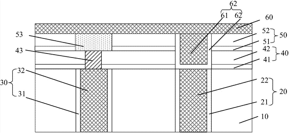
[0032] Please refer to figure 1 , is a schematic structural diagram of a phase change memory.
[0033] The method for forming the phase change memory includes: providing a substrate 10; forming a peripheral metal interconnect structure 20 and a bottom electrode 30 in the substrate 10, the peripheral metal interconnect structure 20 including an interconnect metal layer 22 and an interconnect The bottom electrode 30 includes a bottom electrode metal layer 32 and a bottom electrode adhesive layer 31; a first mask layer 40 is formed on the surface of the substrate 10, and the first mask layer 40 includes a first mask layer 40. A silicon nitride layer 41 and a first silicon oxide layer 42; a first opening is formed in the first mask layer 40, and the first opening exposes part of the surface of the bottom electrode metal layer 32; A bott...
PUM
 Abstract
Description
Claims
Application Information
 - R&D
- Intellectual Property
- Life Sciences
- Materials
- Tech Scout
- Unparalleled Data Quality
- Higher Quality Content
- 60% Fewer Hallucinations
Browse by: Latest US Patents, China's latest patents, Technical Efficacy Thesaurus, Application Domain, Technology Topic, Popular Technical Reports.
© 2025 PatSnap. All rights reserved.Legal|Privacy policy|Modern Slavery Act Transparency Statement|Sitemap|About US| Contact US: help@patsnap.com


