Array base plate and display panel

A technology for array substrates and display areas, which is applied in the fields of instruments, computing, and electrical digital data processing, etc., can solve problems such as electrostatic discharge of touch electrodes, and achieve the effect of preventing electrostatic discharge and avoiding damage

Active Publication Date: 2015-04-29
SHANGHAI TIANMA MICRO ELECTRONICS CO LTD +1
View PDF5 Cites 39 Cited by
  • Summary
  • Abstract
  • Description
  • Claims
  • Application Information

AI Technical Summary

Problems solved by technology

[0007] In view of this, an embodiment of the present invention provides an array substrate and a display panel to solve the technical problem in the prior art that the touch electrodes are charged with static electricity and cause electrostatic discharge between the touch electrodes

Method used


Image

  • Array base plate and display panel
  • Array base plate and display panel
  • Array base plate and display panel

Examples


Embodiment Construction

[0027] The present invention will be further described in detail below in conjunction with the accompanying drawings and embodiments. It should be understood that the specific embodiments described here are only used to explain the present invention, but not to limit the present invention. In addition, it should be noted that, for the convenience of description, only parts related to the present invention are shown in the drawings but not all content.

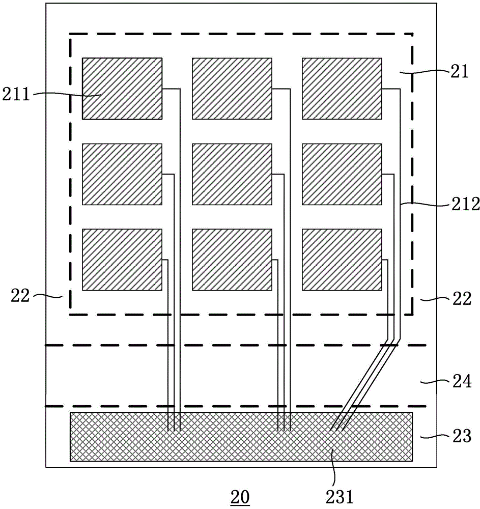
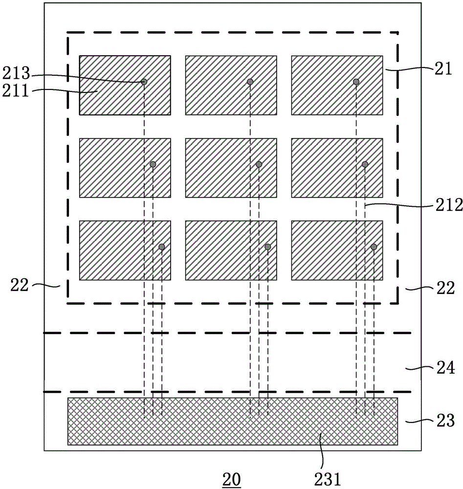
[0028] An embodiment of the present invention provides an array substrate. figure 2 It is a schematic structural diagram of an array substrate provided by an embodiment of the present invention. like figure 2 As shown, the array substrate 20 consists of a display area 21, a frame area 22 surrounding the display area 21, a cutting area 23 located on one side of the frame area 22 (the lower side in the figure), and a cutting area 23 located on the frame area 22. and the stepped area 24 between the cutting area 23, the array ...


PUM


Abstract

The invention discloses an array base plate and a display panel. Through the arrangement of a virtual electrode in a cutting region of the array base plate, and in addition, touch control electrodes are electrically connected with the virtual electrode through a touch control electrode lead wire, so that the touch control electrodes are in short circuit connection, i.e., the voltage difference among the touch control electrodes is zero; or a first electrostatic defending device is arranged in a step region of the array base plate, in addition, the touch control electrodes are electrically connected onto a first short circuit ring through the touch control electrode lead wire and the first electrostatic defending device, when the first electrostatic defending device is switched on through the static electricity of the touch control electrodes, the touch control electrodes conduct the static electricity on the touch control electrodes onto the first short circuit ring through the first electrostatic defending device, and the voltage of the static electricity of the touch control electrodes is reduced. Through the technical scheme provided by the invention, the static electricity discharge among the touch control electrodes can be prevented, so that the damage to the touch control electrodes and the display panel due to the static electricity discharge can be avoided.

Description

technical field [0001] The present invention relates to the field of display technology, in particular to an array substrate and a display panel. Background technique [0002] With the development of modern electronic technology, corresponding components are arranged in the display panel to realize corresponding functions, such as realizing capacitive touch function, etc., so as to bring convenience to users. [0003] At present, according to the formation method of capacitance, capacitive touch can be divided into self-capacitive touch and mutual capacitance touch. Among them, the self-capacitive touch is realized by the capacitance formed between the touch electrode and the ground to realize the touch function, and the mutual capacitance touch Capacitive touch is realized by the capacitance formed between the touch driving electrode and the touch sensing electrode to realize the touch function. [0004] like figure 1 As shown, the display panel 10 is a display panel that...

Claims


Application Information

Patent Timeline
Patent Type & Authority Applications(China)
IPC IPC(8): G06F3/044G02F1/1333
CPCG02F1/13338G02F1/136204G06F3/044G06F2203/04103
Inventor 李嘉灵马从华姚绮君黄忠守
Owner SHANGHAI TIANMA MICRO ELECTRONICS CO LTD
Why Eureka
Try Eureka