Multi-layer flexible film package and liquid crystal display device including the same

a flexible film and liquid crystal display technology, applied in static indicating devices, instruments, cross-talk/noise/interference reduction, etc., can solve problems such as electromagnetic interference, image noise may be generated, liquid crystal panel and driver ics may be damaged, etc., to prevent electrostatic discharge

Inactive Publication Date: 2010-12-28
SAMSUNG DISPLAY CO LTD
View PDF15 Cites 11 Cited by
  • Summary
  • Abstract
  • Description
  • Claims
  • Application Information

AI Technical Summary

Benefits of technology

[0009]An aspect of the present invention is to provide a multi-layer flexible film package which shields electromagnetic waves and prevents electrostatic discharge.
[0010]Another aspect of the present invention is to provide a liquid crystal display device which shields electromagnetic waves and prevents electrostatic discharge, or performs a heat radiation function.
[0011]Still another aspect of the present invention is to provide a liquid crystal display device which shields electromagnetic wave and prevents electrostatic discharge, and at the same time, performs a heat radiation function.

Problems solved by technology

However, the driver ICs generate electromagnetic interference (“EMI”) and electrostatic discharge (“ESD”) due to a plurality of circuit patterns patterned on the flexible film packages.
Further, since a considerable amount of heat is radiated to switch the plurality of electrodes at high speed, a liquid crystal panel and the driver ICs may be damaged or image noise may be generated.

Method used


Image

  • Multi-layer flexible film package and liquid crystal display device including the same
  • Multi-layer flexible film package and liquid crystal display device including the same
  • Multi-layer flexible film package and liquid crystal display device including the same

Examples


Embodiment Construction

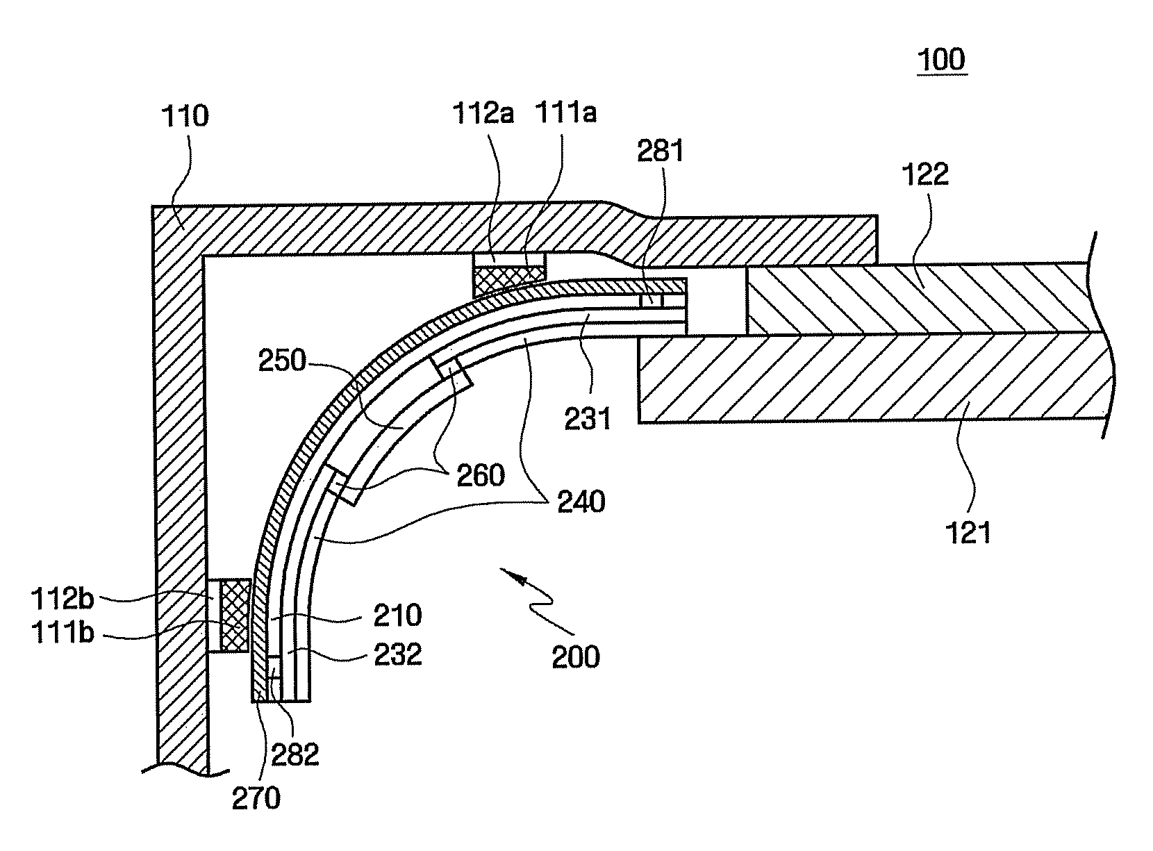
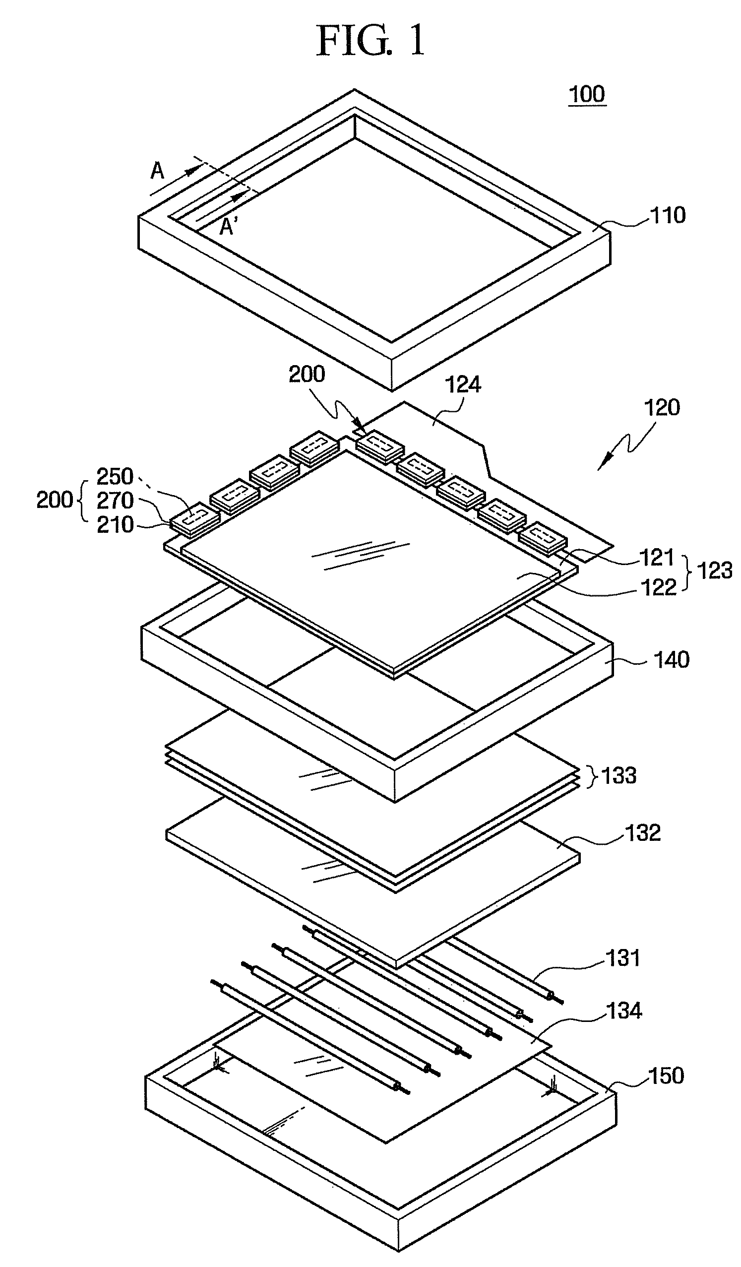
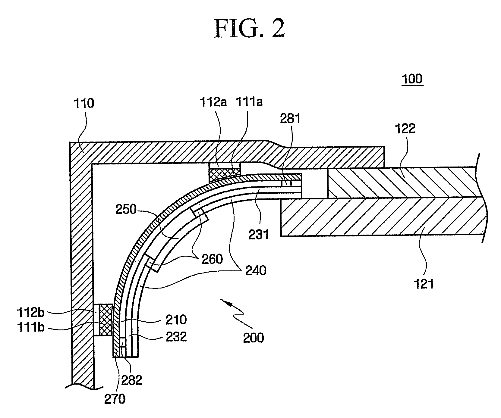
[0029]Advantages, aspects and features of the present invention and methods of accomplishing the same may be understood more readily by reference to the following detailed description of exemplary embodiments and the accompanying drawings. The present invention may, however, be embodied in many different forms and should not be construed as being limited to the exemplary embodiments set forth herein. Rather, these exemplary embodiments are provided so that this disclosure will be thorough and complete and will fully convey the concept of the present invention to those skilled in the art, and the present invention will only be defined by the appended claims. Like reference numerals refer to like elements throughout the specification.

[0030]It will be understood that when an element is referred to as being “on” another element, it can be directly on the other element or intervening elements may be present there between. In contrast, when an element is referred to as being “directly on”...


PUM

PropertyMeasurementUnit
flexibleaaaaaaaaaa
insulatingaaaaaaaaaa
conductiveaaaaaaaaaa

Abstract

A multi-layer flexible film package which shields electromagnetic waves, prevents electrostatic discharge, and at the same time, performs a heat radiation function, and a liquid crystal display device having the same, include an insulating film having circuit patterns and internal ground wiring lines at a first side thereof, an insulating layer formed on the circuit patterns and the internal ground wiring lines, a driver integrated circuit (“IC”) electrically connected to the circuit patterns and the internal ground wiring lines, a ground layer formed on a second side opposite the first side of the insulating film and connected to the internal ground wiring lines, and via holes formed through the insulating film and electrically connecting the internal ground wiring lines and the ground layer.

Description

[0001]This application claims priority to Korean Patent Application No. 10-2006-0072242, filed on Jul. 31, 2006, and all the benefits accruing therefrom under 35 U.S.C. §119, the contents of which in its entirety are herein incorporated by reference.BACKGROUND OF THE INVENTION[0002]1. Field of the Invention[0003]The present invention relates to a multi-layer flexible film package and a liquid crystal display device including the same, and more particularly, to a multi-layer flexible film package which shields electromagnetic waves, prevents electrostatic discharge, and at the same time, performs a heat radiation function, and a liquid crystal display device including the same.[0004]2. Description of the Related Art[0005]A liquid crystal display (“LCD”) device is one of various flat panel displays (FPDs) which are currently widely used. The liquid crystal display device includes two substrates each having electrodes thereon, and a liquid crystal layer interposed between the two subst...

Claims


Application Information

Patent Timeline
Patent Type & Authority Patents(United States)
IPC IPC(8): G02F1/1345
CPCG02F1/13452H01L23/4985H01L23/552H01L23/60H05K1/0218H05K1/189H05K2201/0715H05K2201/09318H05K2201/10681H01L2924/0002H01L2924/00G09G3/20G09G2300/0426G09G2330/06G02F1/1345
Inventor PARK, JOO-HWAN
Owner SAMSUNG DISPLAY CO LTD
Why Eureka
Try Eureka