Method of an array of structures sensitive to ESD and structure made therefrom

a thin film transistor and array technology, applied in the field of fabricating arrays of thin film transistors, can solve the problems of damage to the tft structure, esd is always a big problem, etc., and achieve the effect of avoiding damage from esd during substrate processing

Inactive Publication Date: 2005-08-25
INNOLUX CORP
View PDF4 Cites 13 Cited by
  • Summary
  • Abstract
  • Description
  • Claims
  • Application Information

AI Technical Summary

Benefits of technology

[0008] The present invention provides a solution to avoiding damages from ESD during substrate processing. The individual structures formed on the substrate are initially conductively coupled together by interconnections as the structures are being formed. Electrostatic charges built up in the structures on the substrate are discharge automatically before damage can be done. The interconnections between the individual structures are removed before fabricating another array of structures.

Problems solved by technology

Electrostatic discharge (ESD) is always a big problem with the fabrication of TFT.
Should the electrostatic charges discharge onto the TFT, it would cause arcing, release of a surge of energy, and / or a momentary current and / or voltage surge, which could damage the TFT structure.

Method used


Image

  • Method of an array of structures sensitive to ESD and structure made therefrom
  • Method of an array of structures sensitive to ESD and structure made therefrom
  • Method of an array of structures sensitive to ESD and structure made therefrom

Examples


Embodiment Construction

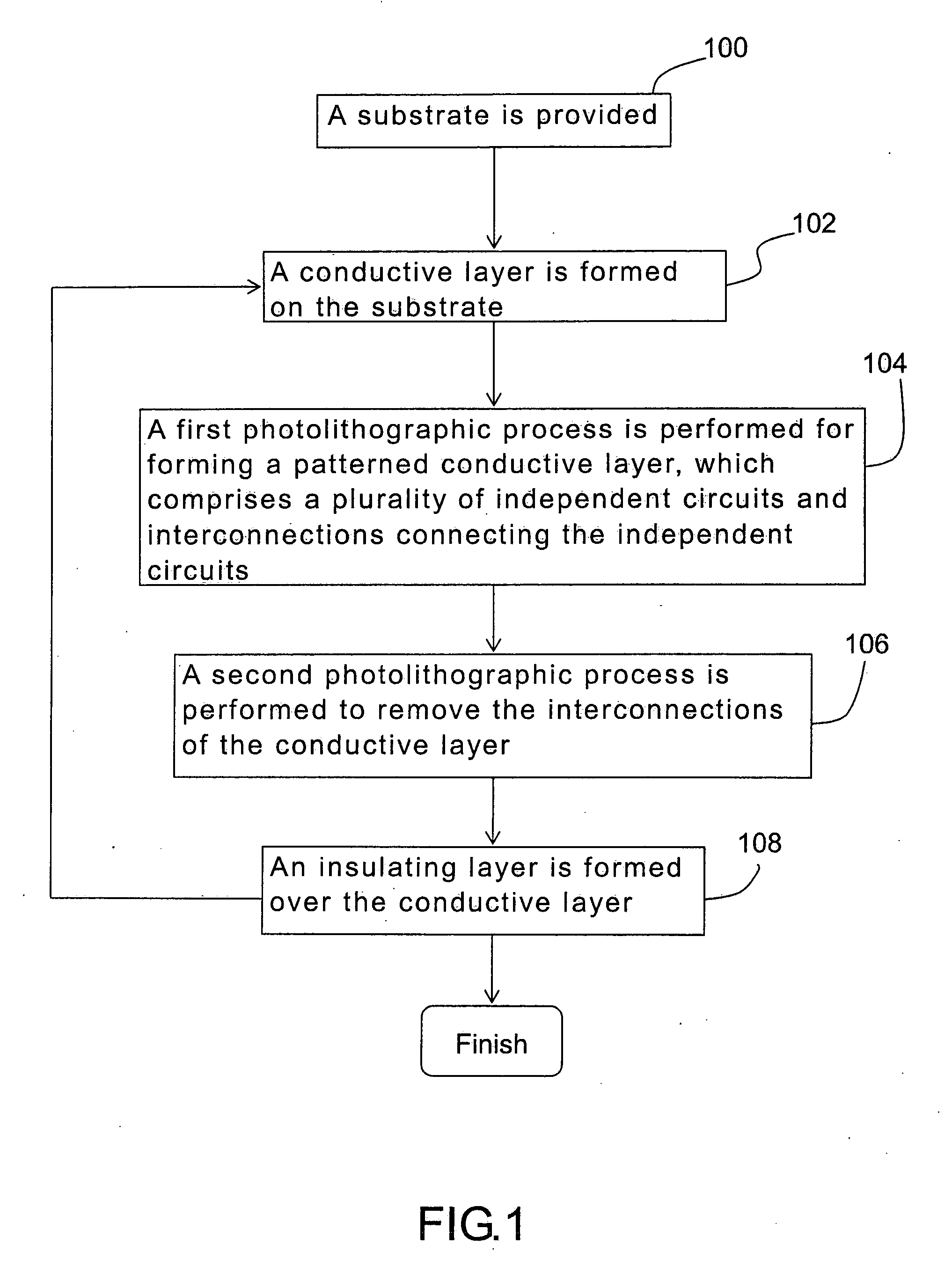
[0019]FIG. 1 is a flow chart illustrating the process flow of fabricating an exemplary TFT array of the present invention. The conductive layer is formed by two photolithographic processes and etching processes. Each photolithographic process includes for example, the steps of photoresist coating, soft bake, hard bake, exposure, fixing, development, and etching to pattern the conductive layer.

[0020] Referring to FIG. 1, a substrate is provided in step 100, which is a transparent substrate, such as, a glass substrate or quartz substrate. In step 102, a conductive layer is formed on the substrate.

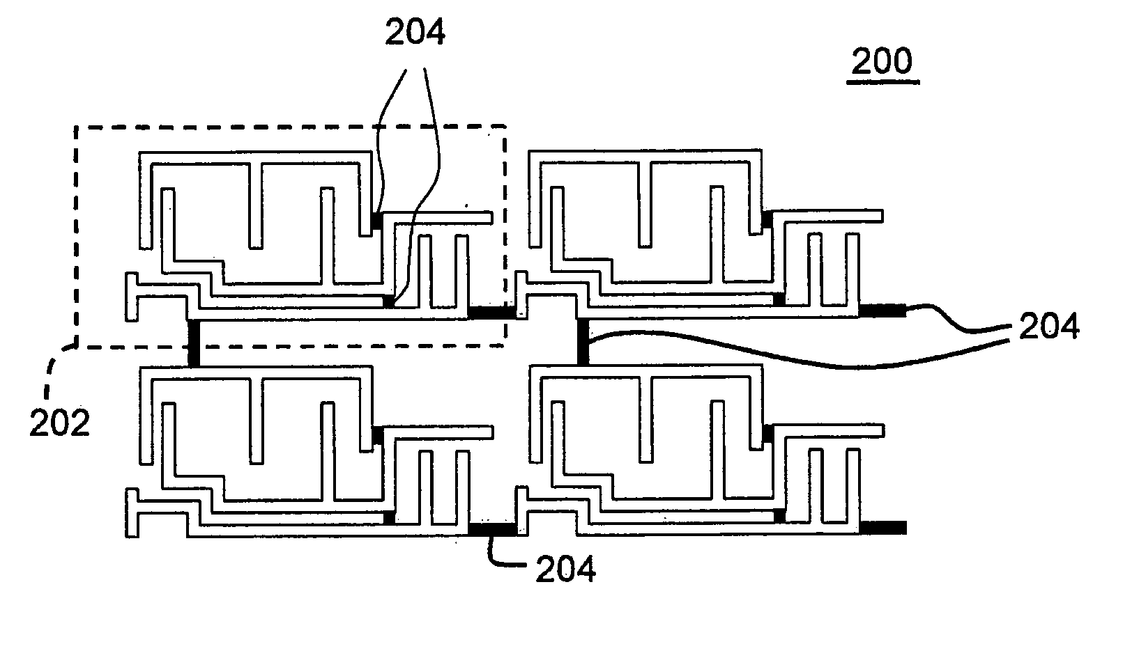
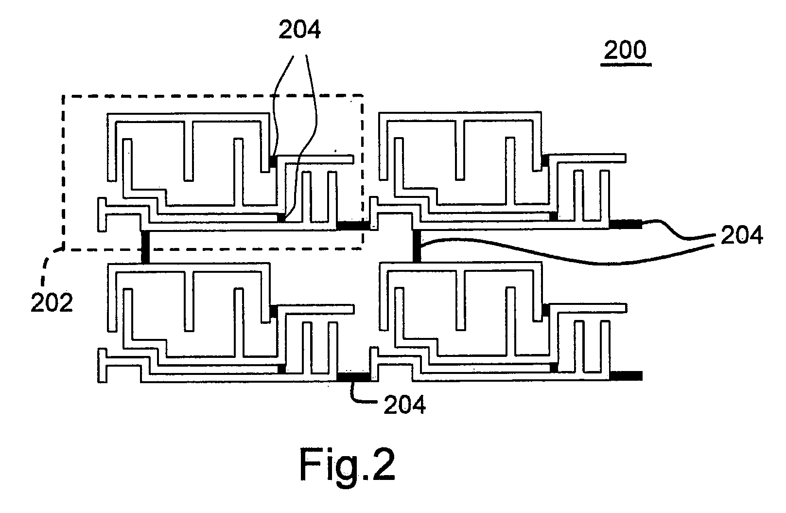
[0021] In step 104, a first photolithographic process is performed for forming a patterned conductive layer, which comprises a plurality of independent circuits and interconnections connecting the independent circuits (see also FIG. 2). Furthermore a point discharge structure can be formed on the edge of the substrate simultaneously (see also FIG. 4). The point discharge structure can reduc...


PUM

PropertyMeasurementUnit
structuresaaaaaaaaaa
electrostatic discharge structureaaaaaaaaaa
electrostatic chargesaaaaaaaaaa

Abstract

A method of fabricating an array of structures sensitive to ESD is disclosed. First, an array of structures is provided on a substrate, with the structures conductively coupled by interconnections. Thereafter, the interconnections are removed before fabricating another array of structures. Therefore, the structures have equal potential. Further, an electrostatic discharge structure is provided near the periphery of the substrates.

Description

CROSS-REFERENCE TO RELATED APPLICATION [0001] This application claims the priority benefit of Taiwan application serial no. 93104404, filed on Feb. 23, 2004. BACKGROUND OF THE INVENTION [0002] 1. Field of the Invention [0003] The present invention relates to a method of fabricating a thin film transistor (TFT) array, and more particularly to a method of fabricating an array of structures sensitive to electrostatic discharge and structure made therefrom. [0004] 2. Description of the Related Art [0005] Because of its low operational voltage, non-radiation, small weight and size superior to those of cathode ray tube (CRT), liquid crystal display, plasma display and electroluminance display have been widely studied and developed, and is viewed as the main stream display in the future. [0006] Active matrix liquid crystal display controls data read / write by active element such as transistors or diodes at pixel, for example, TFT liquid crystal display. When the transistor is on, the signal...

Claims


Application Information

Patent Timeline
Patent Type & Authority Applications(United States)
IPC IPC(8): G02F1/1362G09F9/30H01L21/00G02F1/1368H01L21/28H01L21/3205H01L21/77H01L21/82H01L21/84H01L27/02H01L27/12H01L29/786
CPCG02F1/136204H01L27/1214H01L27/0248
Inventor CHEN, JR-HONGLIN, GWO-LONGCHEN, CHIH-FANG
Owner INNOLUX CORP
Why Eureka
Try Eureka