Semiconductor package and its array arranged substrate structure and production method

An array arrangement, semiconductor technology, applied in the direction of semiconductor/solid-state device manufacturing, semiconductor devices, semiconductor/solid-state device components, etc., can solve the problems of uneven cutting surface, burning cutting surface, irregular shape, etc.

Inactive Publication Date: 2007-10-31
SILICONWARE PRECISION IND CO LTD
View PDF5 Cites 13 Cited by
  • Summary
  • Abstract
  • Description
  • Claims
  • Application Information

AI Technical Summary

Problems solved by technology

[0007] For example, in the semiconductor package disclosed in U.S. Patent Publication 2004/0259291, when the package molding is completed, laser cutting is used to cut the package units arranged in an array to form an irregular Micro SD memory card package. Since the laser cutting path needs to pass through Different materials, such as encapsulation gel, solder repellent layer, conductive circuit, plating bus, etc., can easily cause burning problems on the cutting surface, resulting in irregular shapes and uneven cutting surfaces
[0008] In addition, after the cutting operation is completed, the cutting section of the above-mentioned semiconductor package will expose the conductive lines, which will easily lead to the intrusion of external moisture into the package along the exposed conductive lines, resulting in problems such as a decrease in product reliability.
Furthermore, the conductive circuit exposed by the cutting section is very easy to cause electrostatic current to invade the package due to external electrostatic discharge (ESD), causing damage to the chip.
[0009] Even, in this packaging substrate that utilizes electroplating buses to for...

Method used


Image

  • Semiconductor package and its array arranged substrate structure and production method
  • Semiconductor package and its array arranged substrate structure and production method
  • Semiconductor package and its array arranged substrate structure and production method

Examples


Embodiment 1

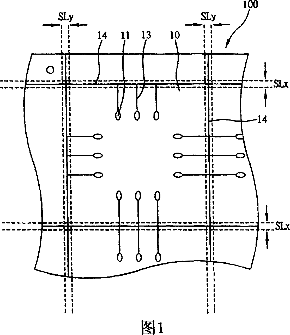
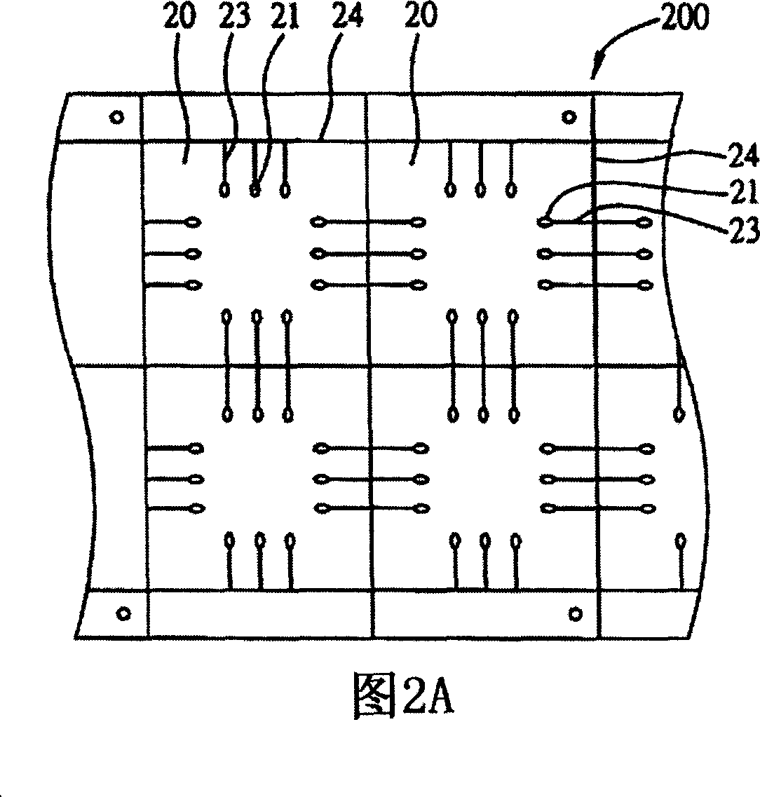
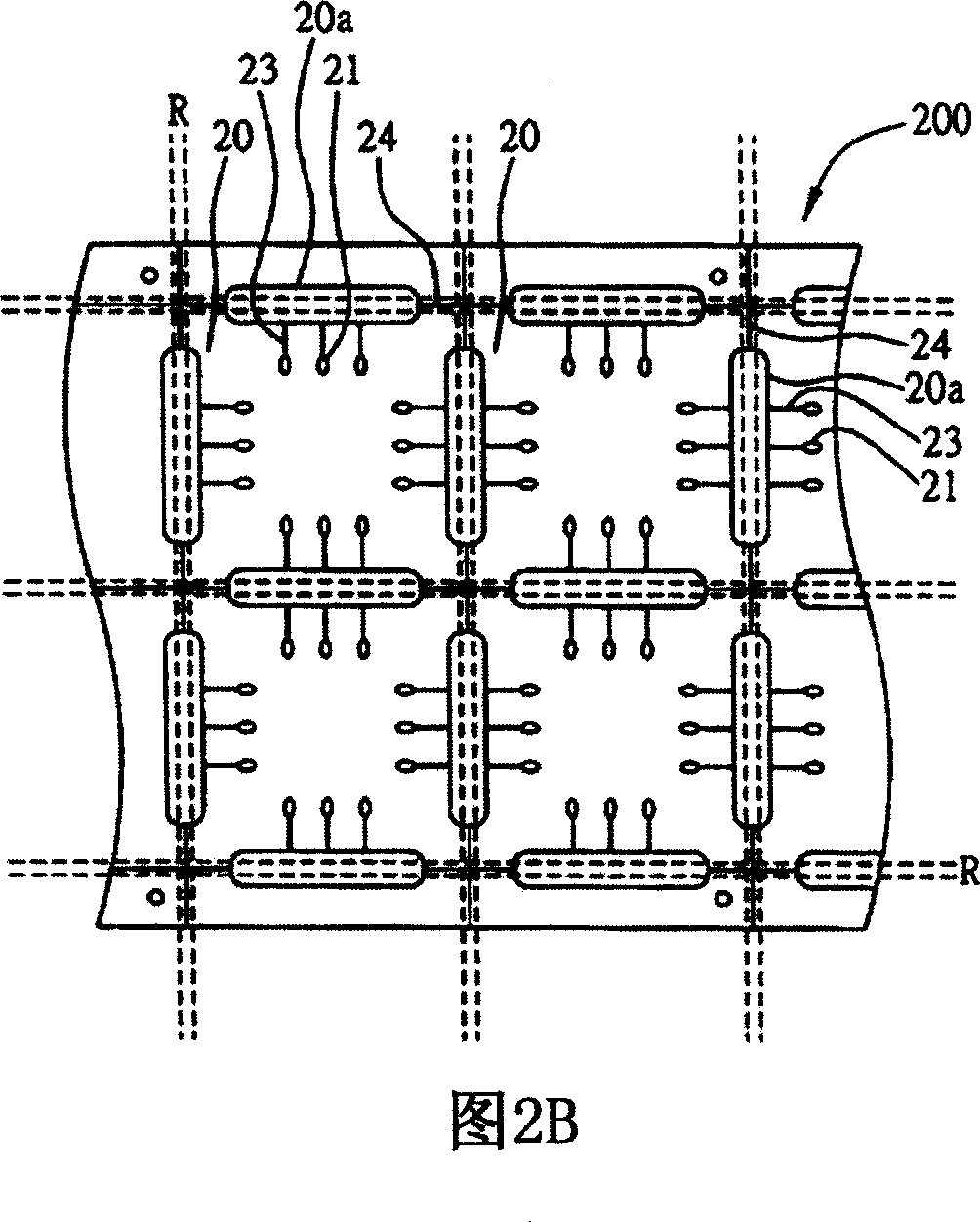
[0031] 2A to 2F are schematic diagrams of Embodiment 1 of the semiconductor package and its array-arranged substrate structure and manufacturing method of the present invention. The semiconductor package may be a thin profile ball grid array (TFBGA) semiconductor package.

[0032] The manufacturing method of the semiconductor package of the present invention is shown in FIG. 2A. First, a substrate 200 is provided, and the substrate sheet 200 includes: a plurality of substrate units 20 arranged in an array, with An electroplating bus 24, and an electrical connection pad 21 is provided in the substrate unit 20, and a conductive circuit 23 electrically connecting the electrical connection pad 21 and the electroplating bus 24, through the electroplating bus 24 and the conductive circuit 23, in An electroplated metal layer (not shown) such as nickel / gold is formed on the electrical connection pad 21 , wherein the electrical connection pad 21 is used for electrical connection betwee...

Embodiment 2

[0039] 3A to 3D are schematic diagrams of Embodiment 2 of the semiconductor package and its manufacturing method of the present invention.

[0040] As shown in Fig. 3A, a substrate 300 is provided, and the substrate 300 includes: a plurality of substrate units 30 arranged in an array, an electroplating bus 34 is provided between the substrate units 30, and in the substrate units 30 An electrical connection pad 31 and a conductive circuit 33 electrically connecting the electrical connection pad 31 and the electroplating bus 34 are provided, and an electroplated metal layer (not shown) is formed on the electrical connection pad 31 through the electroplating bus 34 and the conductive circuit 33. marked).

[0041] As shown in FIG. 3B , slots 30 a are formed between each of the substrate units 30 , and the slots 30 a cut off the connection relationship between the conductive lines 33 and the electroplating bus 34 . The width of the slot 20 a is greater than the width of a dicing l...

Embodiment 3

[0046] 4A to 4B are schematic diagrams of Embodiment 3 of the semiconductor package and its manufacturing method of the present invention. This embodiment is substantially the same as the above-mentioned embodiments, the main difference is that: the semiconductor package and its manufacturing method are applied to the memory card package.

[0047] As shown in Figure 4A, a substrate 400 is provided, and the substrate 400 includes: a plurality of substrate units 40 arranged in an array, each of the substrate units 40 is used to establish a Micro SD memory card package, the substrate unit 40 An electroplating bus 44 is provided between them, and an electrical connection pad 41 is provided in the substrate unit 40, and a conductive circuit 43 electrically connecting the electrical connection pad 41 and the electroplating bus 44 passes through the electroplating bus 44 and conducts electricity. The circuit 43 forms an electroplated metal layer (not shown) on the electrical connecti...


PUM


Abstract

The invention discloses a semiconductor encapsulation piece and substrate structure which is arranged in array and preparation method, the semiconductor encapsulation piece includes: substrate unit part of which forms groove, and plugging compound is filled into the groove; semiconductor chip which is electric connected to the substrate unit; and encapsulation colloid which is formed on the substrate unit and covers the semiconductor chip. When incising along the substrate unit, the incision path passes through the plugging compound or encapsulation colloid, electric detection of substrate unit can be proceeded in advance, it can avoid problem that the material and working procedure are wasted and cost is increased induced by poor product when succeeding steps are accomplished, at the same time, the cutting surface is flat, lead circuit can not be exposed at the cutting surface, it can avoid problems of damage of static and inroad of damp.

Description

technical field [0001] The present invention relates to a semiconductor package and its array-arranged substrate structure and manufacturing method, in particular to an array-arranged substrate structure and manufacturing method with an electroplating bus and its semiconductor package. Background technique [0002] Due to the substantial growth of various portable (Portable) products such as communications, networks, and computers, the area of ​​integrated circuits (ICs) can be reduced, and ball grid array (BGA) packages with high density and multi-pin characteristics have become increasingly popular. Become a mainstream product in the packaging market. The feature of the ball grid array package is that a semiconductor chip is placed on a substrate, and a plurality of solder balls (Solder Ball) arranged in a grid array are arranged on the back of the substrate, so that the same unit area of ​​the semiconductor chip carrier It can accommodate more input / output connection ter...

Claims


Application Information

Patent Timeline
IPC IPC(8): H01L21/50H01L23/498
CPCH01L2924/0002H01L24/97H01L2924/15311H01L2224/48091H01L2224/48227H01L2924/14H01L2924/00014H01L2924/00
Inventor 黄建屏陈建志蔡育杰
Owner SILICONWARE PRECISION IND CO LTD
Why Eureka
Try Eureka