Liquid crystal display device

A technology for liquid crystal display devices and substrates, which is applied to static indicators, instruments, nonlinear optics, etc., can solve the problems of prolonged film formation time of gate insulating layers, decreased glue coating efficiency, and affected production efficiency, and is conducive to miniaturization. And the effect of narrowing the frame, reducing the occupied area, and enhancing the antistatic ability

Active Publication Date: 2012-12-19
SHANGHAI TIANMA MICRO ELECTRONICS CO LTD
View PDF4 Cites 13 Cited by
  • Summary
  • Abstract
  • Description
  • Claims
  • Application Information

AI Technical Summary

Problems solved by technology

[0010] However, increasing the thickness of the gate insulating layer will prolong the film formation time of the gate insulating layer, which will affect the production efficiency, and at the same time, the increase in the thickness of the gate insulating layer will cause a decrease in storage capacitance;
[0011] Reducing the thickness of the first layer of metal will increase the resistance of the metal line, resulting in a decrease in writing ability;
[0012] Partially coating the sealant with conductive particles requires setting multiple sealant nozzles in the corresponding gluing area, resulting in a decrease in gluing efficiency
[0013] How to prevent the drop in yield caused by the tip discharge of conductive particles without affecting other performances of the liquid crystal display device has become an urgent problem to be solved by those skilled in the art

Method used


Image

  • Liquid crystal display device
  • Liquid crystal display device
  • Liquid crystal display device

Examples


Embodiment Construction

[0042] In order to make the above objects, features and advantages of the present invention more comprehensible, specific implementations of the present invention will be described in detail below in conjunction with the accompanying drawings.

[0043] In the following description, many specific details are set forth in order to fully understand the present invention, but the present invention can also be implemented in other ways than those described here, so the present invention is not limited by the specific embodiments disclosed below.

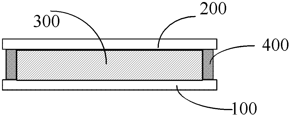
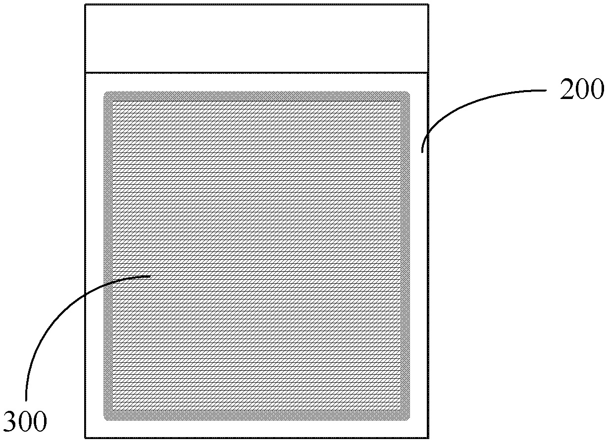
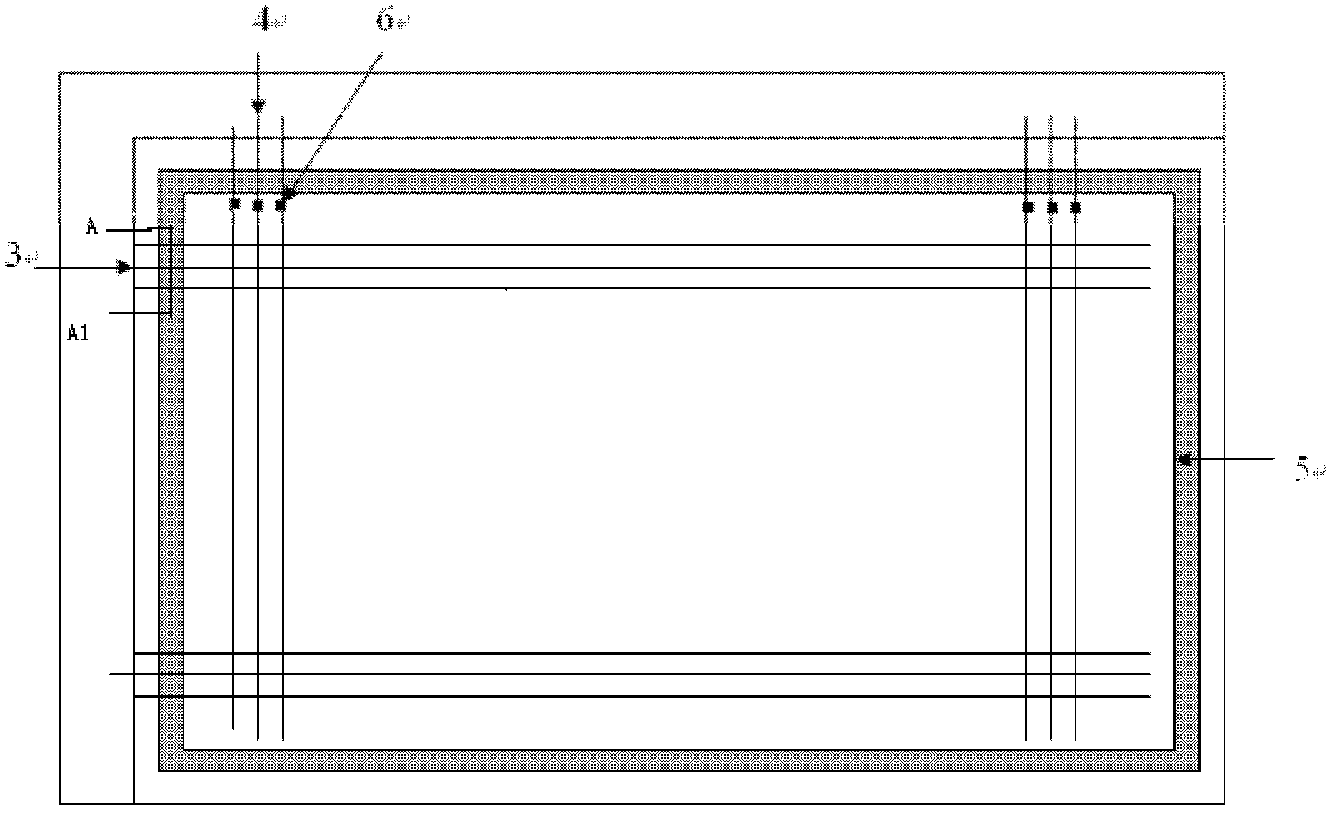
[0044]In order to solve the problems described in the background technology, the inventor provides a liquid crystal display device, comprising: a first substrate, a second substrate, arranged between the first substrate and the second substrate and used for bonding the first substrate and the second substrate Sealing of two substrates, the first substrate is provided with drive lines and first substrate common electrodes facing the directi...


PUM


Abstract

The invention provides a liquid crystal display device which comprises a first substrate, a second substrate and sealing glue, wherein the first substrate and the second substrate are relatively arranged; the sealing glue is arranged between the first substrate and the second substrate for adhering the first substrate and the second substrate; the first substrate is provided with a driving line and a first substrate common electrode toward the direction of the second substrate; the second substrate is provided with a second substrate common substrate toward the direction of the first substrate; a plurality of conductive particles are distributed into the sealing glue; the sealing glue is divided into a first sealing glue area and a second sealing glue; the conductive particles in the first sealing glue area are contacted with the first substrate common electrode and the second substrate common electrode; the conductive particles in the second sealing area are only contacted with the second substrate common electrode; a conductive housing layer is also arranged in the second sealing glue area, and positioned between the conductive parts and the driving line; and a first insulating layer is also arranged between the conductive housing layer and the driving line. With the adoption of the liquid crystal display device, the problems that the yield is reduced due to the discharging of the top ends of the conductive particles can be prevented.

Description

technical field [0001] The invention relates to the field of flat panel display, in particular to a liquid crystal display device. Background technique [0002] Liquid crystal display devices are widely used in various fields due to their small size, light weight, and low radiation. [0003] combined reference figure 1 and figure 2 A cross-sectional view and a plan view of the liquid crystal display device are respectively shown. The liquid crystal display device includes a first substrate 100, a second substrate 200 opposite to the first substrate 100, a liquid crystal layer 300 filled between the first substrate 100 and the second substrate 200, and the first substrate 100 and the second substrate 200 bonded together. The second substrate 200 is sealed with a sealant 400 for the liquid crystal layer 300 . [0004] Currently widely used liquid crystal display modes include Twist Nematics (TN), In Plane Switching (IPS) and Vertical Alignment (VA). Among them, TN mode an...

Claims


Application Information

Patent Timeline
Patent Type & Authority Applications(China)
IPC IPC(8): G02F1/1339G02F1/1362G02F1/133
Inventor 张勤
Owner SHANGHAI TIANMA MICRO ELECTRONICS CO LTD
Why Eureka
Try Eureka