Screen clearing circuit and display device

A display device and circuit technology, applied to static indicators, instruments, etc., can solve the problems of no way to clear the screen, increase power consumption and cost, and achieve the effects of simple structure, residual image removal, and low cost

Active Publication Date: 2015-05-13
KUSN INFOVISION OPTOELECTRONICS
View PDF4 Cites 31 Cited by
  • Summary
  • Abstract
  • Description
  • Claims
  • Application Information

AI Technical Summary

Problems solved by technology

[0004] However, the XON function using Gate Driver IC in the prior art needs to be realized by the IC internal circuit, and requires a screen ...

Method used


Image

  • Screen clearing circuit and display device
  • Screen clearing circuit and display device

Examples


Embodiment Construction

[0020] In order to make the above-mentioned objectives, features and advantages of the present invention more obvious and understandable, the specific embodiments of the present invention will be described in detail below with reference to the accompanying drawings.

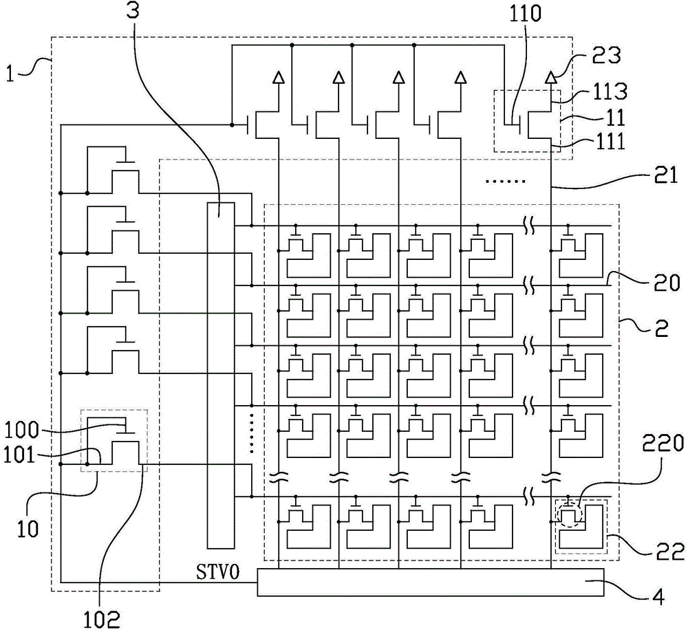
[0021] Please refer to figure 1 , figure 1 It is a schematic diagram of a circuit structure of a display device according to an embodiment of the present invention. Such as figure 1 As shown, the display device includes a clearing circuit 1, a pixel array 2, a gate driving circuit 3, and a source driving circuit 4. The pixel array 2 includes a plurality of scan lines 20, a plurality of data lines 21, and a plurality of pixel switch elements 220 electrically connected to the plurality of scan lines 20 and the plurality of data lines 21, and a plurality of scan lines 20 and a plurality of data lines 21 and a plurality of pixel switching elements 220 constitute a plurality of pixel units 22. The gate driving circuit 3...


PUM


Abstract

The invention provides a screen clearing circuit and a display device. The screen clearing circuit comprises multiple first switch elements and multiple second switch elements. Each first switch element comprises a first control end, a first input end and a first output end, wherein the first control end is connected with the first input end and receives a control signal, each first output end is connected with one scanning line corresponding to a display panel and used for inputting the control signal to the scanning line. Each second switch element comprises a second control end, a second input end and a second output end, wherein the second control end receives the control signal, each second input end is connected with one data line corresponding to the display panel, and the second output end is connected with a public electrode of the display panel. When the display panel normally displays frames, the control signal is a low-level signal. When the display panel is powered off, the control signal is changed into a high-level signal through jumping. The display device can effectively complete screen clearing of the display panel by adopting the screen clearing circuit and is simple in structure and low in cost.

Description

Technical field [0001] The present invention relates to the field of display, in particular to a screen cleaning circuit and a display device adopting the screen cleaning circuit. Background technique [0002] With the popularization of portable products such as smart phones and smart watches, small-size display devices have become more and more integrated into people’s lives due to their powerful operability and superior portability. At the same time, users are more concerned about the display panels of small-size display devices. The requirements are getting higher and higher. As far as the small-size display panel is concerned, during the use of the display panel, when the display panel is scanned line by line from the first line to the last line, in each frame of picture display, each display pixel in the panel keeps displaying this The electric potential required for one frame of picture. Therefore, when the power of the display panel is turned off, each pixel still mainta...

Claims


Application Information

Patent Timeline
IPC IPC(8): G09G3/20
Inventor 陈龙房耸于子阳关佳灵
Owner KUSN INFOVISION OPTOELECTRONICS
Why Eureka
Try Eureka