A kind of oled device manufacturing method and oled device

A device manufacturing method and device technology, which are applied in the fields of semiconductor/solid-state device manufacturing, electric solid-state devices, semiconductor devices, etc., can solve problems such as hindering electron or hole injection, weak carrier injection capability, and difficulty in realizing OLED devices, etc. Achieve the effect of improving lifespan, eliminating impurities and saving manufacturing costs

Active Publication Date: 2017-04-19
TRULY HUIZHOU SMART DISPLAY
View PDF7 Cites 0 Cited by
  • Summary
  • Abstract
  • Description
  • Claims
  • Application Information

AI Technical Summary

Problems solved by technology

[0005] The bidirectional light-emitting device driven by alternating current in the prior art lights up the device by switching positive and negative currents, but its (hole injection layer) HIL and (electron injection layer) EIL are doped according to a certain ratio to achieve both Injecting electrons can also inject holes. When (hole injection layer) HIL and (electron injection layer) EIL are doped together, some reactions may occur, hindering the injection of electrons or holes, so its carrier injection ability is very weak, it is very difficult to realize the AC-driven OLED device

Method used


Image

  • A kind of oled device manufacturing method and oled device
  • A kind of oled device manufacturing method and oled device
  • A kind of oled device manufacturing method and oled device

Examples


Embodiment 1

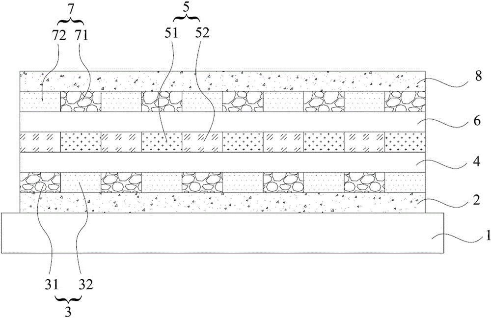
[0067] An OLED device, comprising a substrate 100 and at least one pixel located on the substrate 100, the pixel comprising:

[0068] anode 200;

[0069] cathode 800;

[0070] An organic functional layer located between the anode 200 and the cathode 800; the organic functional layer includes a first injection layer 300, a first transport layer 400, a light emitting layer 500, a second transport layer 600 and a second Injection layer 700; wherein,

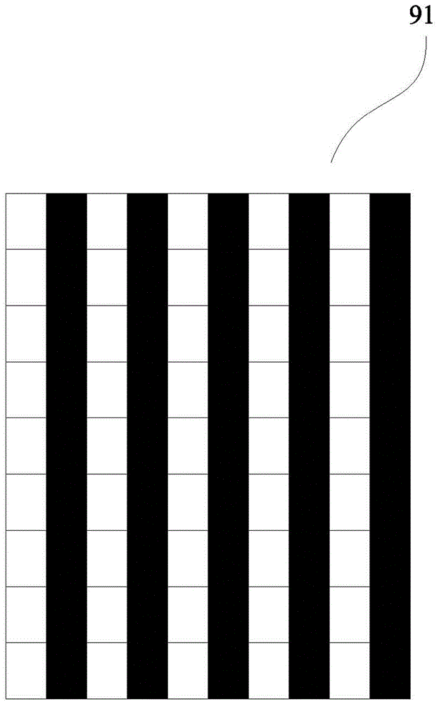
[0071] The first injection layer 300 includes five first hole injection strips 310 and five first electron injection strips 320, the first hole injection strips 310 and the first electron injection strips 320 are arranged in parallel adjacent to each other;

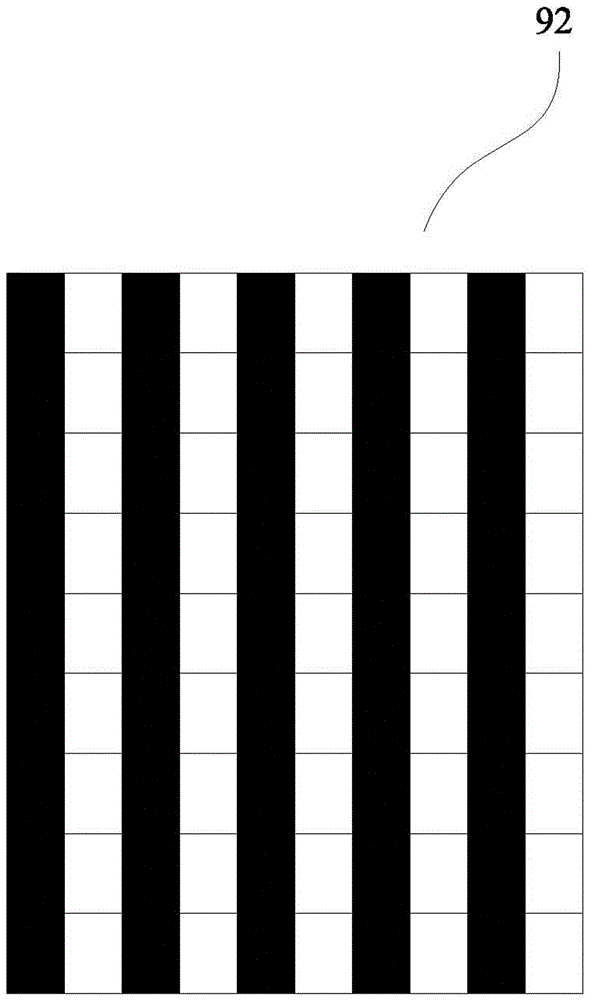
[0072] The second injection layer 700 includes five second hole injection strips 710 and five second electron injection strips 720, the second hole injection strips 710 and the second electron injection strips 720 are arranged in parallel adjacent to each other, the The seco...

Embodiment 2

[0090] An OLED device, comprising a substrate 100 and at least one pixel located on the substrate 100, the pixel comprising:

[0091] anode 200;

[0092] cathode 800;

[0093] An organic functional layer located between the anode 200 and the cathode 800; the organic functional layer includes a first injection layer 300, a first transport layer 400, a light emitting layer 500, a second transport layer 600 and a second Injection layer 700; wherein,

[0094] The first injection layer 300 includes five first hole injection strips 310 and five first electron injection strips 320, the first hole injection strips 310 and the first electron injection strips 320 are arranged in parallel adjacent to each other;

[0095] The second injection layer 700 includes five second hole injection strips 710 and five second electron injection strips 720, the second hole injection strips 710 and the second electron injection strips 720 are arranged in parallel adjacent to each other, the The seco...

Embodiment 3

[0113] Please refer to Figure 6 , an OLED device, comprising a substrate 100 and at least one pixel located on the substrate 100, the pixel comprising:

[0114] anode 200;

[0115] cathode 800;

[0116] An organic functional layer located between the anode 200 and the cathode 800; the organic functional layer includes a first injection layer 300, a first transport layer 400, a light emitting layer 500, a second transport layer 600 and a second Injection layer 700; wherein,

[0117] The first injection layer 300 includes five first hole injection strips 310 and five first electron injection strips 320, the first hole injection strips 310 and the first electron injection strips 320 are arranged in parallel adjacent to each other;

[0118] The second injection layer 700 includes five second hole injection strips 710 and five second electron injection strips 720, the second hole injection strips 710 and the second electron injection strips 720 are arranged in parallel adjacent...


PUM


Abstract

The invention discloses a method for manufacturing an OLED device and an OLED device. The OLED device comprises an anode; a cathode; an organic functional layer located between the anode and the cathode; A first transport layer, at least one light-emitting layer, a second transport layer, and a second injection layer; wherein, the first injection layer includes at least one first hole injection strip and at least one first electron strip that are adjacent in parallel and arranged in series Injection strips; the second injection layer includes at least one second hole injection strip and at least one second electron injection strip that are adjacent in parallel and arranged in series. The second electron injection strip and the second hole injection strip are respectively connected to the The first hole injection strip and the first electron injection strip are arranged opposite to each other. The monochrome or white light area corresponding to the first hole injection strip is first lit by alternating current. After the positive and negative switching, the monochrome or white area corresponding to the first electron injection strip is lit in a short time. The time is short, and the human eye can only see it. The entire monochromatic or white emitting layer.

Description

technical field [0001] The invention relates to the fields of display and lighting, in particular to a method for manufacturing an organic electroluminescent device (OLED device) and the OLED device. Background technique [0002] Organic Light-Emitting Diodes (OLED for short) is a self-luminous device, which has light weight, ultra-thin, high theoretical luminous efficiency, and more importantly, it can be made flexible, whether it is lighting or display, It will be the direction of future development. [0003] The efficiency and lifespan of organic light-emitting materials have been greatly improved. Especially in recent years, the photoelectric properties of red and green organic light-emitting materials have fully met the requirements of industrialization, but the efficiency of blue light materials is still very low, and the lifespan is still very low. It is also very low, especially in the case of high voltage and long-time lighting devices, the life and efficiency deca...

Claims


Application Information

Patent Timeline
Patent Type & Authority Patents(China)
IPC IPC(8): H01L51/56H01L51/50H01L51/52
CPCH10K50/171H10K50/17H10K50/00H10K71/00
Inventor 苏圣勋蔡晓义柯贤军苏君海黄亚清李建华
Owner TRULY HUIZHOU SMART DISPLAY
Why Eureka
Try Eureka