Integrated circuit packaging method

A packaging method and integrated circuit technology, applied in circuits, electrical components, electrical solid devices, etc., can solve problems such as metal stress cracking in the PAD area, and achieve the effect of solving metal cracking

Inactive Publication Date: 2015-05-27
SHANGHAI HUAHONG GRACE SEMICON MFG CORP
View PDF2 Cites 2 Cited by
  • Summary
  • Abstract
  • Description
  • Claims
  • Application Information

AI Technical Summary

Problems solved by technology

[0004] The technical problem to be solved by the present invention is to provide an integrated circuit packaging method to solve the problem of cracking caused by metal stress in the PAD area

Method used


Image

  • Integrated circuit packaging method
  • Integrated circuit packaging method
  • Integrated circuit packaging method

Examples


Embodiment Construction

[0020] The integrated circuit packaging method of the present invention comprises the following steps:

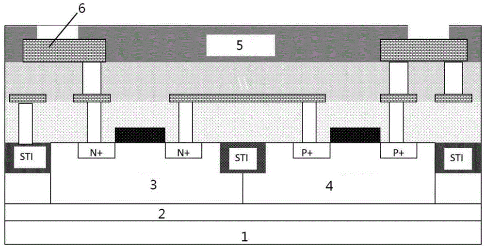
[0021] The first step is to deposit a thin layer of top layer metal on the silicon wafer with a thickness of 0.2-2.0 μm, and open the PAD window of the passivation layer by photolithography after forming the passivation layer. Such as figure 2 shown.

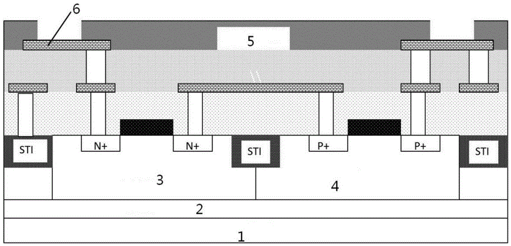
[0022] In the second step, a thicker layer of metal is deposited by CVD, with a thickness of 0.5-5.0 μm, and the material is aluminum / copper, or copper, or other materials. Such as image 3 shown.

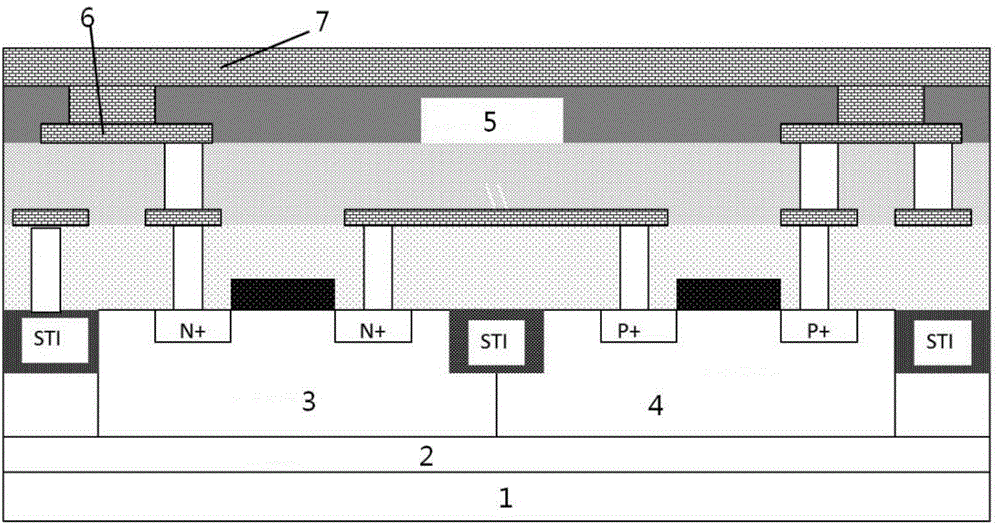
[0023] The third step is to remove the metal outside the PAD window on the passivation layer. The removal process may be a reverse etching plus CMP process, or a photolithography and etching process. If the photolithography plus etching process is used, the mask plate with the same passivation layer is used to form a photoresist with opposite characteristics to the passivation layer, that is, the positive photoresist used wh...


PUM


Abstract

The invention discloses an integrated circuit packaging method which comprises the following steps: step 1, thinner top metal is deposited, and a passivation layer PAD window is defined and opened through photoetching after the passivation layer is formed; step 2, a metal layer is deposited again; and step 3, metal except the PAD window on the passivation layer is removed. The metal strength in a PAD area is reinforced selectively, and the metal on other wired areas is kept thinner, so that the problem of cracking of metal in the PAD area due to packing wire bonding stress is solved under the condition that the wiring density is not influenced.

Description

technical field [0001] The invention relates to the field of semiconductor integrated circuit manufacturing, in particular to an integrated circuit packaging method. Background technique [0002] In the current technology, when the integrated circuit device is packaged, the integrated circuit PAD metal and the metal pin of the outer frame are connected through gold wires. When packaging and wiring, the metal wire has a relatively large compressive stress acting on the metal layer at the PAD of the chip. Such as figure 1 As shown, if the metal layer is thin, it is very likely that the stress will crack the metal layer when the package is wired. In severe cases, the layer below the metal layer will also crack, affecting product performance. [0003] In order to avoid metal cracking, the current general method is to increase the thickness of the metal. For example, the current metal layer thickness of the BCD700V process is 1.5 μm. However, after increasing the metal thickne...

Claims


Application Information

Patent Timeline
IPC IPC(8): H01L25/065H01L21/60
Inventor 王惠惠金锋
Owner SHANGHAI HUAHONG GRACE SEMICON MFG CORP
Why Eureka
Try Eureka