Gate Protection Caps and Method of Forming the Same

A technology of protective cover and gate, applied in electrical components, circuits, semiconductor devices, etc., can solve problems such as reducing the yield of integrated circuits

Active Publication Date: 2015-05-27
TAIWAN SEMICON MFG CO LTD
View PDF4 Cites 4 Cited by
  • Summary
  • Abstract
  • Description
  • Claims
  • Application Information

AI Technical Summary

Problems solved by technology

However, the decrease in minimum feature size and increase in density can lead to pr...

Method used


Image

  • Gate Protection Caps and Method of Forming the Same
  • Gate Protection Caps and Method of Forming the Same
  • Gate Protection Caps and Method of Forming the Same

Examples


Embodiment Construction

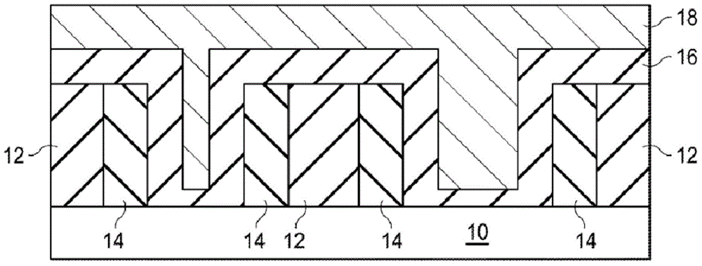
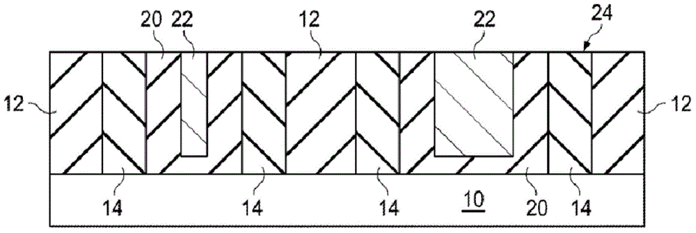
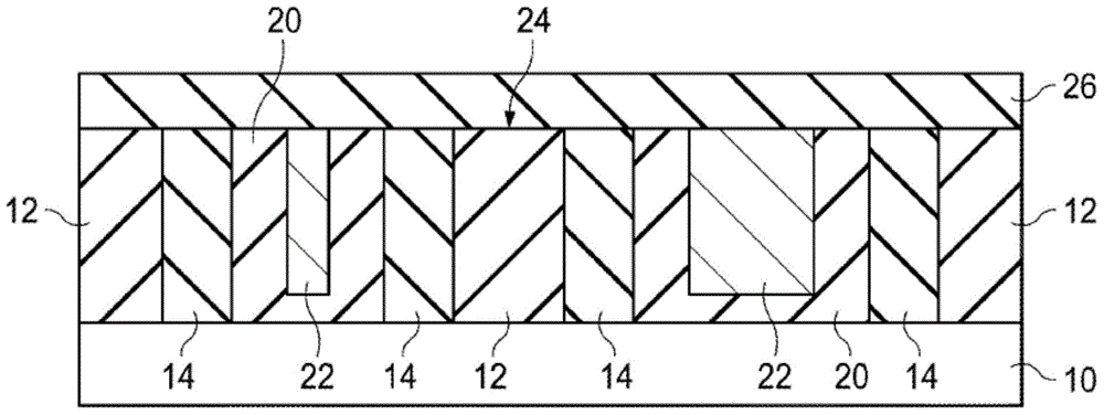
[0048] The making and using of this embodiment are discussed in detail below. It should be appreciated, however, that the present invention provides many applicable concepts that can be embodied in a wide variety of specific contexts. The specific embodiments discussed are merely illustrative of specific ways to make and use the disclosed subject matter, and do not limit the scope of the various embodiments.

[0049] Embodiments will be described with reference to a specific context, namely, a gate-last process for forming transistors, such as fin field effect transistors (FinFETs). However, other embodiments may also apply to other structures and processes. Throughout the drawings and the following discussion, like reference numbers refer to like components. Although the methods discussed herein are described as being performed in a particular order, other method embodiments may be performed in any logical order. Furthermore, it will be apparent to those of ordinary skill ...


PUM


Abstract

A structure includes a substrate, a gate structure over the substrate, a dielectric layer over the substrate, and a cap over a gate electrode of the gate structure. Top surfaces of the dielectric layer and gate electrode are co-planar. The gate structure extends a gate lateral distance between first and second gate structure sidewalls. The cap extends between first and second cap sidewalls. A first cap portion extends from a midline of the gate structure laterally towards the first gate structure sidewall and to the first cap sidewall a first cap lateral distance, and a second cap portion extends from the midline laterally towards the second gate structure sidewall and to the second cap sidewall a second cap lateral distance. The first cap lateral distance and the second cap lateral distance are at least half of the gate lateral distance.

Description

technical field [0001] The invention relates to the field of semiconductors, in particular to a gate protection cover and a forming method thereof. Background technique [0002] The semiconductor industry has experienced rapid growth due to continuous improvements in the integration density of various electronic components (eg, transistors, diodes, resistors, capacitors, etc.). This improvement in integration density comes primarily from iterative reductions in minimum feature size (e.g., shrinking semiconductor process nodes toward the sub-20nm node), which allows more components to be integrated into a given area. The resulting increased integration density generally results in improved integrated circuits, such as integrated circuits with reduced delay. However, the decrease in minimum feature size and increase in density can cause problems in manufactured integrated circuits that can reduce the yield of the integrated circuits. Contents of the invention [0003] In v...

Claims


Application Information

Patent Timeline
IPC IPC(8): H01L29/423H01L21/28
CPCH01L21/28247H01L29/66545H01L21/76897H01L21/76834H01L21/823468H01L21/823864H01L27/0296H01L29/785H01L21/823437H01L21/28008H01L29/4232H01L29/6656
Inventor 林志翰林志忠张铭庆陈昭成
Owner TAIWAN SEMICON MFG CO LTD
Why Eureka
Try Eureka