


Quick Research
Generate reliable direction feasibility study reports for your R&D in just a few steps.

Technical Q&A
Discover and master advanced knowledge NOW. Basics, ideas, possibilities, all at once.

Find Solutions
As an expert in R&D theories, this can generate solutions to your technical problems instantly.

Evaluate Feasibility
Analyze your overall solution with one click, know your potential R&D risks in advance.

Monitor Landscape
Get weekly tech updates, stay abreast of the latest tech innovations and key insights.
Method for doping semiconductor substrates
A semiconductor and substrate technology, applied in the field of doped semiconductor substrates
- Summary
- Abstract
- Description
- Claims
- Application Information
AI Technical Summary
Problems solved by technology
Method used
Image

Examples
Embodiment Construction
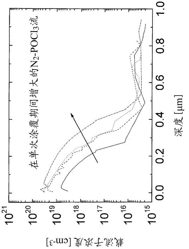
[0042] in figure 1 In, how to simultaneously change the concentration of dopants in a plurality of regions near the surface of the semiconductor substrate and the diffusion depth of the dopants in the semiconductor substrate is described with reference to the schematic diagram. By adding the dopant source (here POCl 3 ) Increase the gas flow, and the result is to simultaneously change the dopant concentration and the dopant diffusion depth in multiple regions near the surface. Therefore, according to the prior art, separate adjustment of these two parameters is impossible.
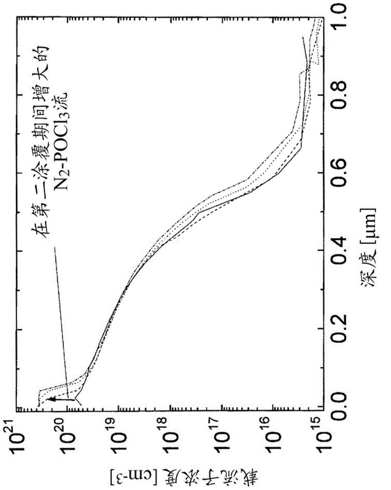
[0043] in figure 2 Here, the second coating stage according to the method according to the invention is shown with reference to the schematic diagram. As a result, it can be detected that the concentration of dopants in multiple regions close to the surface can be changed without changing the diffusion depth of the dopants.
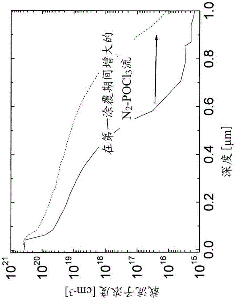
[0044] in image 3 Here, the first coating stage of the method according to the inv...
PUM
 Abstract
Description
Claims
Application Information
 - R&D Engineer
- R&D Manager
- IP Professional
- Industry Leading Data Capabilities
- Powerful AI technology
- Patent DNA Extraction
Browse by: Latest US Patents, China's latest patents, Technical Efficacy Thesaurus, Application Domain, Technology Topic, Popular Technical Reports.
© 2024 PatSnap. All rights reserved.Legal|Privacy policy|Modern Slavery Act Transparency Statement|Sitemap|About US| Contact US: help@patsnap.com