
Matrix circuit substrate, display apparatus, and manufacturing method of matrix circuit substrate

A circuit substrate and display device technology, which is applied in static indicators, nonlinear optics, optics, etc., can solve the problems of the display device not being light enough, beautiful, and the increase in volume of the touch display device, and achieve narrow frame area and space reduction The effect of using

Inactive Publication Date: 2015-06-03
BARCO TAIWAN TECH +1
View PDF4 Cites 12 Cited by
  • Summary
  • Abstract
  • Description
  • Claims
  • Application Information

AI Technical Summary

Problems solved by technology

[0005] However, the space reserved by the periphery of the matrix circuit substrate for the bonding of external pins increases the frame width of the display device, which makes the display device not light and beautiful in terms of visual perception, and the display panel and the touch panel need to be connected separately. A flexible circuit board, so it will increase the size of the touch display device

Method used


Image

  • Matrix circuit substrate, display apparatus, and manufacturing method of matrix circuit substrate
  • Matrix circuit substrate, display apparatus, and manufacturing method of matrix circuit substrate
  • Matrix circuit substrate, display apparatus, and manufacturing method of matrix circuit substrate

Examples


Embodiment Construction

[0075] The matrix circuit substrate, the display device and the manufacturing method of the matrix circuit substrate according to the preferred embodiments of the present invention will be described below with reference to the relevant drawings, wherein the same elements will be described with the same reference symbols. The drawings of all the embodiments of the present invention are for illustration only, and do not represent real dimensions and proportions.

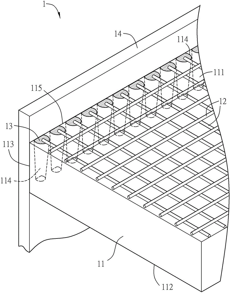
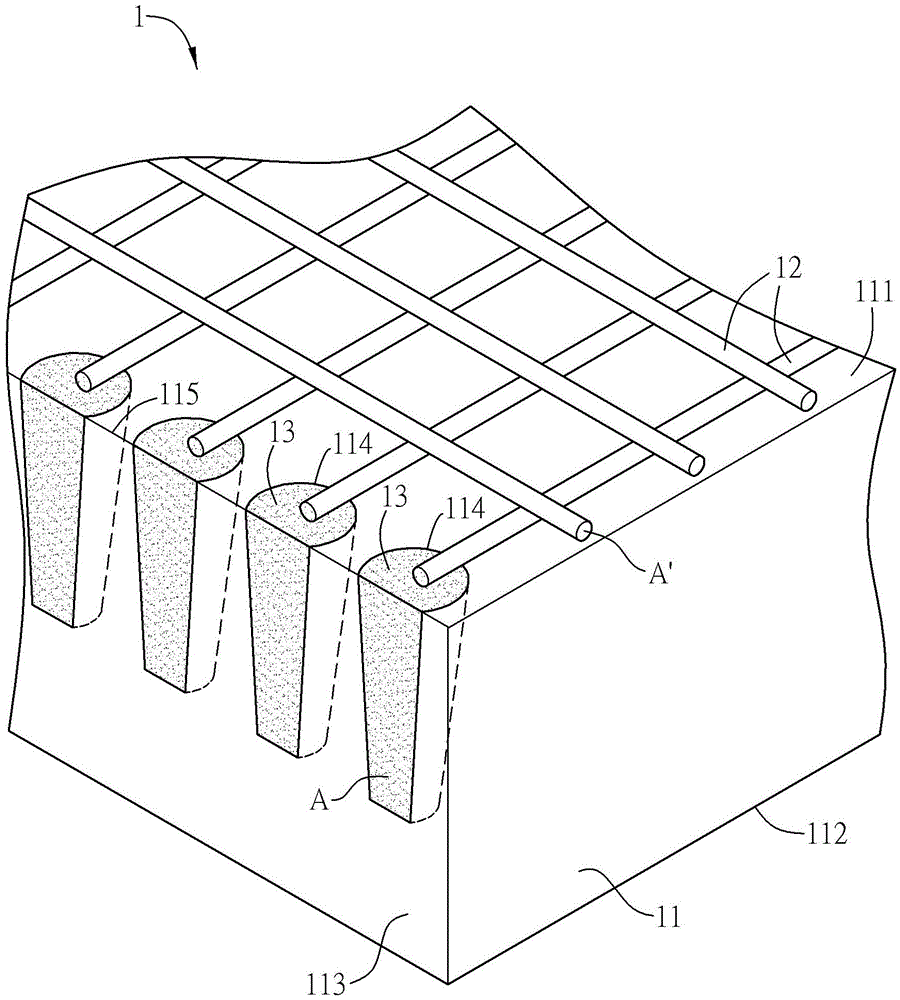
[0076] Figure 1A It is a partial schematic diagram of a matrix circuit substrate according to the first embodiment of the present invention, such as Figure 1A As shown, the matrix circuit substrate 1 includes a substrate body 11 , a plurality of electrodes 12 and at least one first conductive material 13 . Wherein, the material of the matrix circuit substrate 1 can include resin, metal, ceramics, glass, plastic or other light-transmitting materials, which can be applied to various display panels, such as TFT substrate...


PUM


Abstract

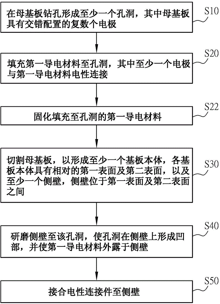
A matrix circuit substrate includes a substrate body, multiple electrodes and at least one first conductive material. The substrate body has a first surface and a second surface which are opposite each other, and at least one sidewall located between the first surface and the second surface, the sidewall having at least one recess. The multiple electrodes are disposed in a crisscross manner on the first surface. The first conductive material is disposed in the recess to correspond to at least one of the electrodes, and electrically connected to the electrode. The invention also discloses a display apparatus and a method for manufacturing a matrix circuit substrate.

Description

technical field [0001] The invention relates to a matrix circuit substrate. Background technique [0002] With the advancement of science and technology, various information devices are constantly being introduced, especially various types of display devices or touch display devices, which are used in various electronic devices, such as mobile phones, tablet computers, ultra-thin notebooks, electronic books etc. Both the display device and the touch layer are composed of a matrix circuit substrate. [0003] Generally speaking, the matrix circuit substrate has electrodes arranged in a staggered manner, and is electrically connected to the driving circuit board through a flexible printed circuit (FPC), and connected to an external control chip. As far as the display device is concerned, the flexible circuit board is connected to an external control chip to control the light emission of each pixel of the display panel to display a picture. In addition, in terms of a touch-se...

Claims


Application Information

Patent Timeline
IPC IPC(8): G02F1/133G02F1/163G02F1/167
CPCG02F1/13452G02F1/13338G02F1/13454G02F2201/42
Inventor 吴永良彼得里昂约翰-玛莉吉瑞兹史文亚历山卓史洽尔
Owner BARCO TAIWAN TECH
Learn More