Fan-out-type wafer level package method

A wafer-level packaging and fan-out technology, which is applied in the manufacture of electrical components, electrical solid-state devices, semiconductor/solid-state devices, etc., can solve the problems of increased packaging costs and achieve easy control, fast and easy interconnection, and simplified process flow Effect

Active Publication Date: 2015-06-03
江苏中科智芯集成科技有限公司
View PDF4 Cites 33 Cited by
  • Summary
  • Abstract
  • Description
  • Claims
  • Application Information

AI Technical Summary

Problems solved by technology

from figure 2 In terms of packaging structure, in this method, since the conductive bumps of the chip are not exposed outside the plastic package, additional polishing is required in the process to lead out the I / O, resulting in increased packaging costs

Method used


Image

  • Fan-out-type wafer level package method
  • Fan-out-type wafer level package method
  • Fan-out-type wafer level package method

Examples


Embodiment Construction

[0016] The technical solutions in the embodiments of the present invention will be clearly and completely described below with reference to the accompanying drawings in the embodiments of the present invention. Obviously, the described embodiments are only a part of the embodiments of the present invention, but not all of the embodiments. Based on the embodiments of the present invention, all other embodiments obtained by those of ordinary skill in the art without creative efforts shall fall within the protection scope of the present invention.

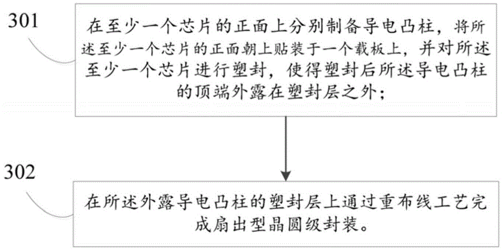
[0017] image 3 Shown is a flow chart of a fan-out wafer-level packaging method according to an embodiment of the present invention. like image 3 As shown, the method includes:

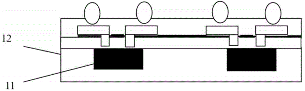
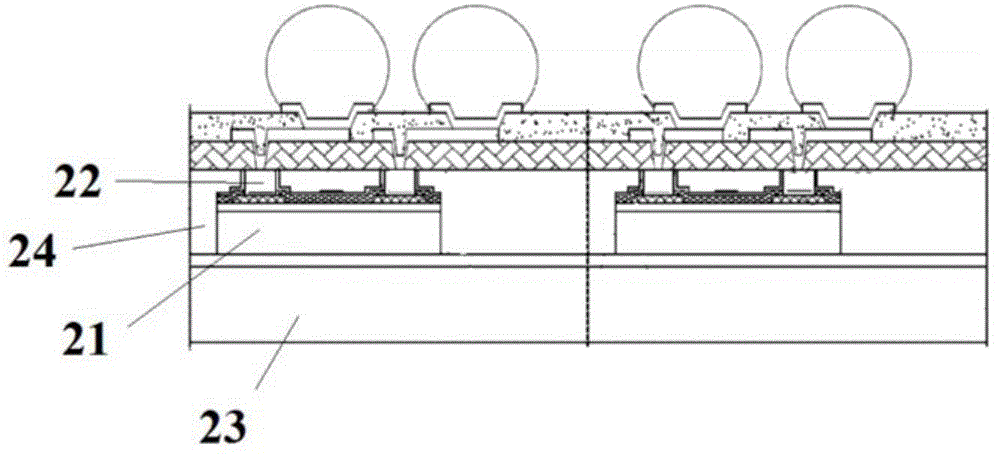
[0018] Step 301: Prepare conductive bumps on the front side of at least one chip, mount the at least one chip on a carrier board with the front side facing up, and plastic-encapsulate the at least one chip, so that the conductive bumps after plastic-encaps...


PUM


Abstract

The embodiment of the invention provides a fan-out-type wafer level package method which is applicable to a small thin chip, and the technological process is simplified. The fan-out-type wafer level package method comprises the following steps of preparing a conductive convex column on the front surface of at least one chip, upwards mounting the front surface of the at least one chip on a carrier plate, and performing plastic package on the at least one chip, so that after plastic package, the top end of the conductive convex column is exposed to the outside of a plastic package body; and finishing the fan-out-type wafer level package on the plastic package body with the exposed conductive convex column by virtue of a rewiring technology.

Description

technical field [0001] The invention relates to the technical field of semiconductor packaging, in particular to a fan-out wafer-level packaging method. technical background [0002] Fan Out Wafer Level Package (FOWLP for short) is a wafer-level processing embedded chip packaging method. One of the advanced packaging methods with better flexibility. Existing common FOWLP technologies include the eWLP package invented by Infineon Technologies AG and the TSMC FOWLP package invented by TSMC. [0003] figure 1 Shown is a schematic structural diagram of an Infineon eWLP package in the prior art. like figure 1 As shown, this packaging method is to mount the chip 11 on the carrier board with the front side facing down, and then plastic-encapsulate the chip 11 in the plastic package 12 . Since the front side of the chip 11 faces the carrier after plastic sealing, in order to expose the conductive electrodes on the front side of the chip 11 for the rewiring process, the carrier ...

Claims


Application Information

Patent Timeline
Patent Type & Authority Applications(China)
IPC IPC(8): H01L21/56H01L21/60
CPCH01L21/561H01L21/568H01L21/6835H01L23/3114H01L23/482H01L24/19H01L24/96H01L24/97H01L2221/68372H01L2224/12105H01L2924/18162H01L2924/3511H01L2924/00H01L21/56H01L24/10H01L24/11H01L24/12H01L2224/11H01L2224/12
Inventor 王宏杰刘一波陈峰上官东恺孙鹏
Owner 江苏中科智芯集成科技有限公司
Why Eureka
Try Eureka