Solid-state imaging device, manufacturing method of solid-state imaging device, and electronic device

A technology of solid-state imaging devices and imaging pixels, which is applied in the direction of electric solid-state devices, radiation control devices, circuits, etc., and can solve the problems of reduced sensitivity and difficulty in focusing

Active Publication Date: 2020-05-19
SONY CORP
View PDF6 Cites 0 Cited by
  • Summary
  • Abstract
  • Description
  • Claims
  • Application Information

AI Technical Summary

Problems solved by technology

[0007] However, when the sensitivity of the imaging pixels is optimized, the sensitivity of the phase difference detection pixels decreases, and especially when the subject is dark, it is difficult to accurately perform focusing

Method used


Image

  • Solid-state imaging device, manufacturing method of solid-state imaging device, and electronic device
  • Solid-state imaging device, manufacturing method of solid-state imaging device, and electronic device
  • Solid-state imaging device, manufacturing method of solid-state imaging device, and electronic device

Examples


Embodiment Construction

[0059] Hereinafter, embodiments of the present technology will be described with reference to the drawings.

[0060] Construction example of a solid-state imaging device

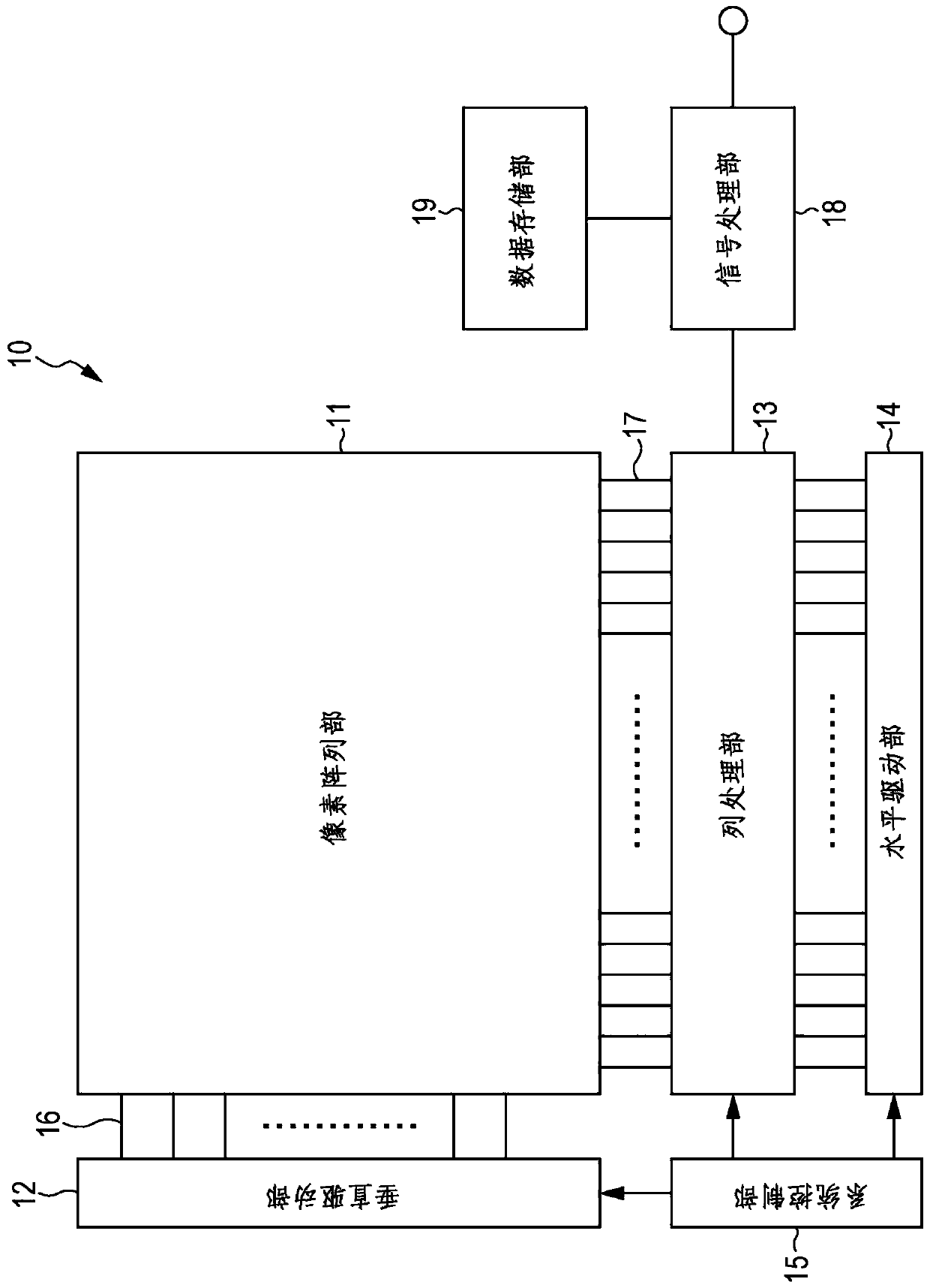
[0061] figure 1 is a block diagram showing an example of a solid-state imaging device to which the present technology is applied. Hereinafter, the configuration of a surface-irradiated type complementary metal oxide semiconductor (CMOS: complementary metal oxide semiconductor) image sensor, which is an amplification type solid-state imaging device, will be described. This technology is not limited to being applied to a surface-illuminated CMOS image sensor, but can also be applied to a back-illuminated CMOS image sensor, other amplifying solid-state imaging devices, or images such as a charge coupled device (CCD: charge coupled device) Sensors and other charge transport solid-state imaging devices.

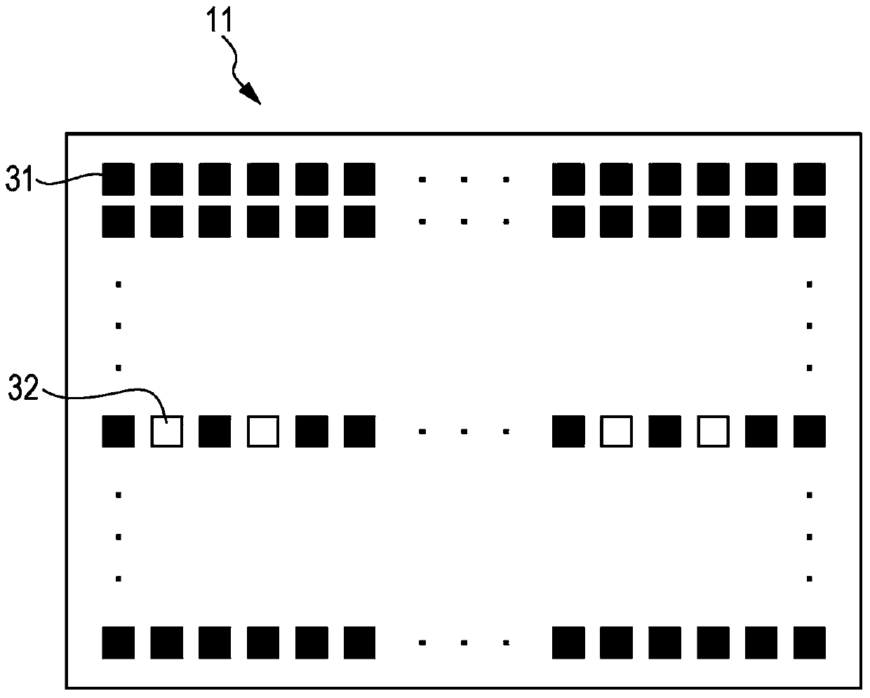
[0062] figure 1 The illustrated CMOS image sensor 10 includes: a pixel array unit 11 formed on a semicond...


PUM


Abstract

The invention provides a solid-state imaging device, a manufacturing method of the solid-state imaging device, and electronic equipment. The solid-state imaging device includes: an imaging pixel including a photoelectric conversion portion that receives incident light; and a phase difference detection pixel including the photoelectric conversion portion and a light shielding portion that blocks light incident on the photoelectric conversion portion. part of the light. In the solid-state imaging device, the imaging pixel further includes a high-refractive index film formed on the upper side of the photoelectric conversion portion, and the phase difference detection pixel further includes a film formed on the upper side of the photoelectric conversion portion. side of the low-refractive index film. The present invention can optimize the sensitivity of the imaging pixels and the AF performance of the phase difference detection pixels.

Description

technical field [0001] The present technology relates to a solid-state imaging device, a method of manufacturing a solid-state imaging device, and an electronic device, and more particularly, to a solid-state imaging device capable of optimizing the sensitivity of imaging pixels and the AF (autofocus) performance of a phase difference detection pixel, a solid-state imaging device, and a solid-state imaging device. Device manufacturing method and electronic device. Background technique [0002] In the related art, various techniques have been proposed for solid-state imaging devices in order to improve sensitivity or prevent color mixing. [0003] For example, a solid-state imaging device has been proposed in which, in each pixel, as a diverging lens (the diverging lens allows the condensing point of incident light from an on-chip lens (on-chip lens) to approach the light-receiving surface) A lens layer is formed in which a portion corresponding to the center of the light re...

Claims


Application Information

Patent Timeline
Patent Type & Authority Patents(China)
IPC IPC(8): H01L27/146
CPCH01L27/14627H01L27/14621H01L27/14685H01L27/14623H01L27/1462H01L27/14636H01L27/14645H04N25/40
Inventor 关勇一井上俊徳狭山征博中元幸香
Owner SONY CORP
Why Eureka
Try Eureka