CMOS image sensor device and its formation method
An image sensor and pattern technology, which is applied in radiation control devices, electric solid devices, semiconductor devices, etc., can solve the problems such as the inability of the lens to focus, achieve the effect of optimizing the sensitivity and improving the forming method
- Summary
- Abstract
- Description
- Claims
- Application Information
AI Technical Summary
Problems solved by technology
Method used
Image
Examples
Embodiment Construction
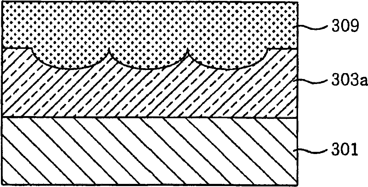
[0018] example figure 2 is a view showing the structure of a CIS device according to an embodiment of the present invention. A photoresist (hereinafter, PR) is coated over the entire surface of the top of the logic part 301 including a photodiode over the semiconductor substrate. Then, a barrier layer for forming an MLA pattern and a PR pattern are sequentially formed over the entire surface of the PR top. The MLA pattern is formed by performing an etching process to selectively remove the barrier layer deposited over the entire surface. The MLA PR pattern 303a is formed by performing isotropic etching using the PR pattern as a mask and then using the MLA pattern as a mask.
[0019] Next, an MLA having a concave structure may be manufactured by filling the material 309 into the entire surface of the top of the MLA PR pattern 303a and performing a planarization process. Material 309 has a refractive index n 2 Higher than the refractive index of the MLA PR pattern 303a.
...
PUM
 Abstract
Description
Claims
Application Information


