Package Structure Of Light Emitting Diode

A technology for light-emitting diodes and packaging structures, applied in electrical components, electrical solid-state devices, circuits, etc., can solve problems such as damage, increase in electronic components, and shorten the service life of light-emitting diodes, and achieve the effect of improving heat dissipation efficiency and solving heat dissipation problems.

Inactive Publication Date: 2015-06-24
GENESIS PHOTONICS
View PDF4 Cites 2 Cited by
  • Summary
  • Abstract
  • Description
  • Claims
  • Application Information

AI Technical Summary

Problems solved by technology

[0002] When electronic products are in operation, the current in the circuit will generate unnecessary heat energy due to flowing through the impedance. If the heat energy cannot be effectively removed and accumulated on the electronic components inside the electronic product, the electronic components may be affected by the rising temperature. damage due to temperature
Therefore, the heat dissipation efficiency greatly affects the operation of electronic products.
Especially for light-emitting diodes, when the temperature of light-emitting diodes increases, the luminous efficiency of light-emitting diodes will decrease significantly, and the service life of light-emitting diodes will be shortened

Method used


Image

  • Package Structure Of Light Emitting Diode
  • Package Structure Of Light Emitting Diode
  • Package Structure Of Light Emitting Diode

Examples


Embodiment Construction

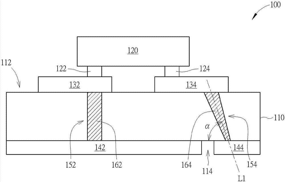
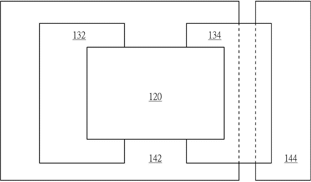
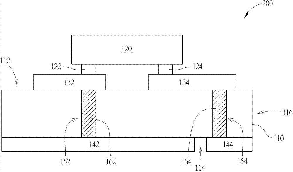
[0012] Please also refer to figure 1 and figure 2 . figure 1 It is a schematic diagram of the first embodiment of the package structure of the light emitting diode of the present invention. figure 2 It is a schematic diagram of the orthographic area configuration of related components of the light emitting diode packaging structure of the present invention on a substrate 110 . like figure 1 As shown, the LED packaging structure 100 of the present invention includes a substrate 110 and a LED die 120 . The substrate 110 has an opposite upper surface 112 and a lower surface 114 . The upper surface 112 of the substrate is provided with two upper metal pads 132 , 134 which are not conductive to each other. The lower surface 114 of the substrate is provided with two lower metal pads 142 , 144 which are not electrically connected to each other. The LED die 120 straddles the upper metal pads 132 , 134 . The LED chip 120 has a first electrode 122 and a second electrode 124 ele...


PUM


Abstract

A package structure of light emitting diode includes a substrate and a light emitting diode die. The substrate has an upper surface and a lower surface opposite to each other. Two upper metal pads without mutual conduction are arranged on the upper surface. Two lower metal pads without mutual conduction are arranged on the lower surface. The light emitting diode die is disposed across the two upper metal pads. The light emitting diode die has a first electrode and a second electrode electrically connected to the two upper metal pads respectively. Wherein an orthographic projection area of one of the lower metal pads is greater than or equal to an orthographic projection area of the light emitting diode die, and the orthographic projection area of the light emitting diode die is totally located within the orthographic projection area of one of the lower metal pads.

Description

technical field [0001] The invention relates to a packaging structure of a light emitting diode, in particular to a packaging structure of a light emitting diode that can improve heat dissipation efficiency. Background technique [0002] When electronic products are in operation, the current in the circuit will generate unnecessary heat energy due to flowing through the impedance. If the heat energy cannot be effectively removed and accumulated on the electronic components inside the electronic product, the electronic components may be affected by the rising temperature. damage due to temperature. Therefore, the heat dissipation efficiency greatly affects the operation of electronic products. Especially for light-emitting diodes, when the temperature of the light-emitting diodes increases, the luminous efficiency of the light-emitting diodes will decrease significantly, and the service life of the light-emitting diodes will be shortened. As light-emitting diodes are gradua...

Claims


Application Information

Patent Timeline
Patent Type & Authority Applications(China)
IPC IPC(8): H01L33/62
CPCH01L33/486H01L33/62H01L2224/48091H01L2933/0066H01L2924/00014H01L33/642
Inventor 黄靖恩苏柏仁吴志凌丁绍滢黄逸儒罗玉云
Owner GENESIS PHOTONICS
Why Eureka
Try Eureka