Display device and pixel circuit and display driving method thereof

A pixel circuit, bias current technology, applied in circuits, electrical components, electrical solid devices, etc., can solve the problem of only light-emitting stage, LCD display driving method without compensation stage, etc., to achieve the effect of fast data input

Active Publication Date: 2015-07-15
PEKING UNIV SHENZHEN GRADUATE SCHOOL
View PDF5 Cites 13 Cited by
  • Summary
  • Abstract
  • Description
  • Claims
  • Application Information

AI Technical Summary

Problems solved by technology

figure 2 The display driving method indicated is generally called progressive light-emitting technology, which is the same as the current disp

Method used


Image

  • Display device and pixel circuit and display driving method thereof
  • Display device and pixel circuit and display driving method thereof
  • Display device and pixel circuit and display driving method thereof

Examples


Embodiment 1

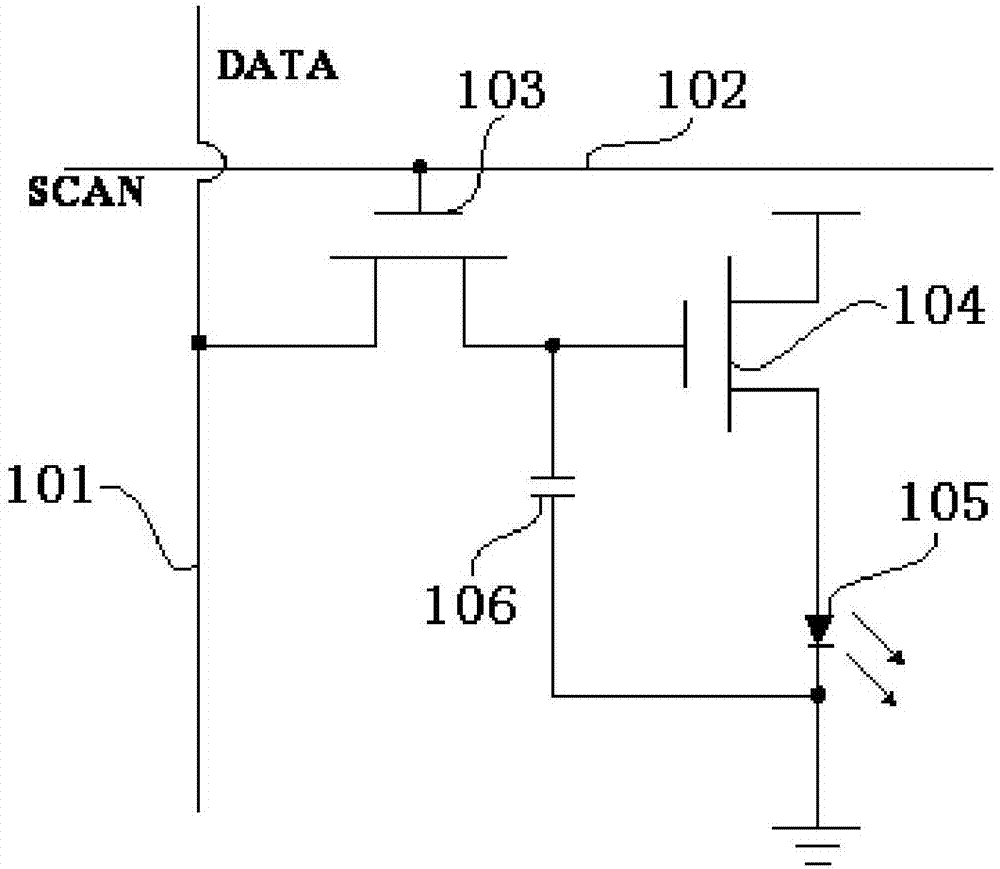
[0052] Please refer to Figure 4 , this embodiment provides a pixel circuit, including a light emitting element 40 , a driving transistor 41 , a first switching transistor 42 , a second switching transistor 43 , a first capacitor 44 and a second capacitor 45 .

[0053] The control electrode of the driving transistor 41 is coupled to the storage node 47 , the first electrode is coupled to the bias current terminal, and the second electrode is coupled to the light emitting element 40 . When the light emitting element 40 is an OLED, the second electrode of the driving transistor 41 is coupled to the anode of the OLED, and the cathode of the OLED is coupled to the common electrode VSS.

[0054] The control electrode of the first switch transistor 42 is coupled to the first scanning signal terminal, the first electrode is coupled to the bias current terminal, and the second electrode is coupled to the storage node 47 .

[0055] The control electrode of the second switch transistor...

Embodiment 2

[0078] Please refer to Figure 7 , this embodiment provides another pixel circuit, including a light emitting element 70 , a driving transistor 71 , a first switching transistor 72 , a second switching transistor 73 , a first capacitor 74 and a second capacitor 75 .

[0079] The control electrode of the driving transistor 71 is coupled to the storage node 77 , the first electrode is coupled to the bias current terminal, and the second electrode is coupled to the light emitting element 70 . When the light emitting element 70 is an OLED, the second electrode of the driving transistor 71 is coupled to the anode of the OLED, and the cathode of the OLED is coupled to the common electrode VSS.

[0080] The control electrode of the first switch transistor 72 is coupled to the first scanning signal terminal, the first electrode is coupled to the bias current terminal, and the second electrode is coupled to the storage node 77 .

[0081] The control electrode of the second switch tran...

Embodiment 3

[0102] Please refer to Figure 10 , corresponding to Embodiment 1, this embodiment provides a display device, including a display panel 102 , a data driving circuit 103 and a gate driving circuit 106 .

[0103] The display panel 102 is composed of N*M pixel circuits 101 provided in Embodiment 1 arranged in a matrix, where N is the number of rows of the display panel 102, M is the number of columns of the display panel 102, and M and N are positive integers .

[0104] The data drive circuit 103 includes M bias current lines 104 and M data signal lines 105, and the bias current lines 104 are respectively connected to the bias current terminals of the pixel circuits 101 in each column (that is, the bias current terminals of the same column of pixel circuits are connected to to the same bias current line) for providing bias current and driving voltage to the pixel circuit 101; the data signal line 105 is respectively connected to the data signal end of each column of pixel circui...


PUM


Abstract

The invention provides a display device and a pixel circuit and a display driving method thereof. According to the display device and the pixel circuit thereof, threshold voltage information of a driver transistor and a light-emitting element is extracted from a threshold extraction frame in a current bias manner, and data voltage is written into a driving frame in a capacitive coupling manner, so that driving current passing through the light-emitting element is irrelevant to the threshold voltage information, threshold voltage drift of both transistors and the light-emitting element or nonuniformity of threshold voltage of all the transistors of a display panel is accurately compensated, and grey information (data voltage) is written in a voltage programming manner to realize quick data input. Besides, in the display driving method, one display driving period is divided into one threshold extraction frame and a plurality of driving frames, so that the ratio of the lighting time to the threshold extraction time of the light-emitting element is increased.

Description

technical field [0001] The present application relates to a display device, a pixel circuit thereof, and a display driving method. Background technique [0002] Organic Light-Emitting Diode (OLED) display has been extensively studied in recent years due to its advantages of high brightness, high luminous efficiency, wide viewing angle and low power consumption, and has been rapidly applied to a new generation of displays. OLED display driving methods include passive matrix driving (Passive Matrix OLED, PMOLED) and active matrix driving (Active Matrix OLED, AMOLED). Although the cost of passive matrix driving is low, there is crosstalk phenomenon, which cannot realize high-resolution display, and the passive matrix driving current is large, which reduces the service life of OLED. In contrast, the active matrix driving method sets a different number of transistors on each pixel as a current source, which avoids crosstalk, requires less driving current, and lower power consump...

Claims


Application Information

Patent Timeline
IPC IPC(8): G09G3/32H01L27/32G09G3/3258
Inventor 张盛东冷传利王翠翠
Owner PEKING UNIV SHENZHEN GRADUATE SCHOOL
Why Eureka
Try Eureka