Pixel circuit, display device and display driving method
A technology of pixel circuit and display device, applied in the field of display device and display driver, pixel circuit, can solve the problems of complex circuit structure, reduction of pixel aperture ratio, increase of line cost, etc., to achieve fast data input, reduce production cost, simple circuit effect of structure
- Summary
- Abstract
- Description
- Claims
- Application Information
AI Technical Summary
Problems solved by technology
Method used
Image
Examples
Embodiment 1
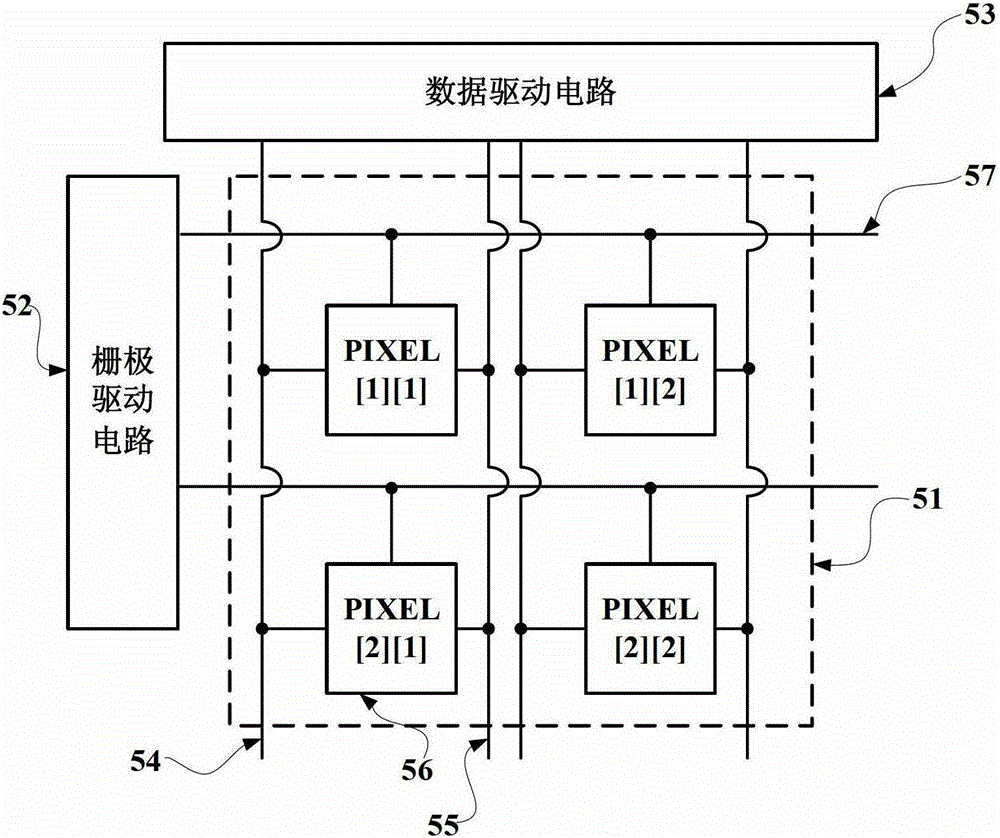
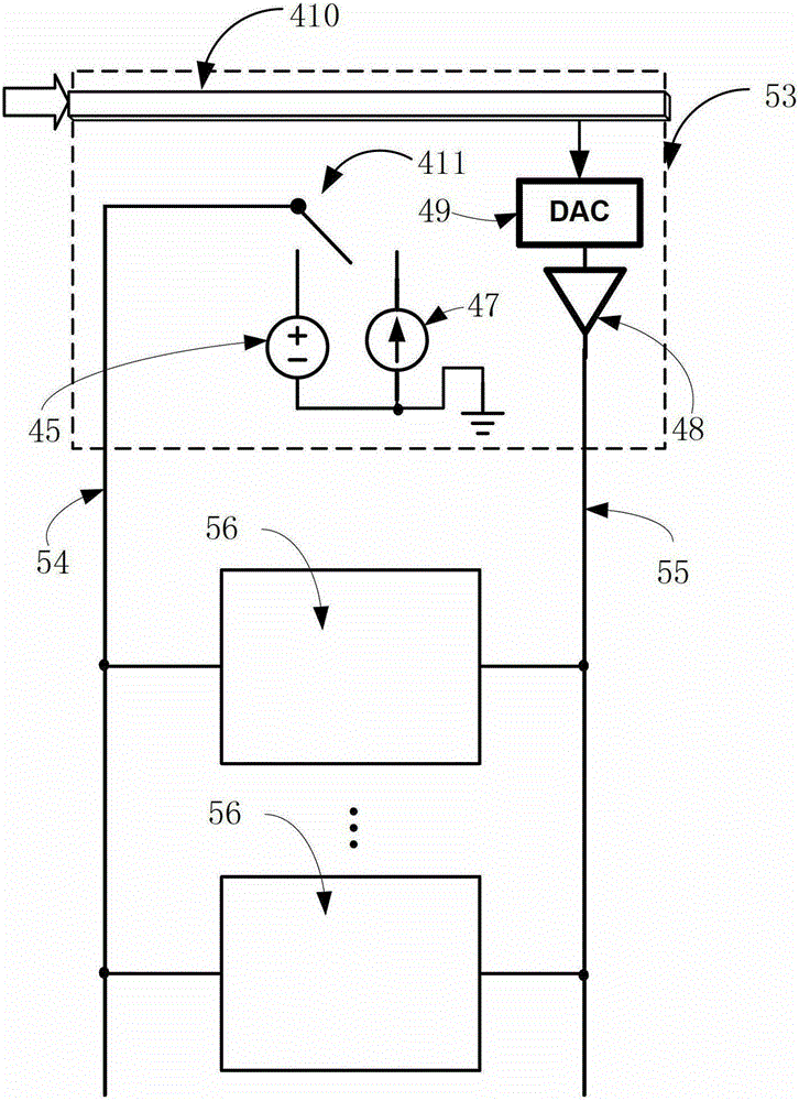
[0049] Please refer to figure 2 , figure 2 The structure of the display device according to the first embodiment of the present application is shown, which mainly includes a display panel, a gate driving circuit 52 and a data driving circuit 53 . The display panel includes several pixel arrays 51 . Wherein, the pixel array 51 is composed of N rows and M columns of pixel circuits 56 arranged in a matrix, that is, the pixel array 51 has N rows and M columns, where N and M are both positive integers. Generally, the pixel circuits 56 in the same row in the pixel array 51 are connected to the same scan line 57 , and the pixel circuits 56 in the same column in the pixel array 51 are connected to the same data line 55 and bias current line 54 . The gate driving circuit 52 is used to provide scanning signals to the pixel circuits 56 through the scanning lines 57 . The data driving circuit 53 is used to provide grayscale information to the pixel circuit through the data line 55, t...
Embodiment 2
[0078] Please refer to Figure 6 , the main difference from Embodiment 1 is that in the display device, the gate drive circuit 52 also provides a control line 64 whose level is opposite to that of the scanning line in the data input stage, and the pixel circuit 56 mainly includes: an organic light emitting diode 29 as The light-emitting element, the first capacitor 27, the first transistor 24 provided with the first control electrode, the first electrode and the second electrode as a switch control module, and the second transistor 24 provided with the second control electrode, the third electrode and the fourth electrode The transistor 25 serves as a driving module. For convenience, a storage node 68 (that is, the first terminal of the first capacitor 27 ) is set here. The first control electrode is coupled to the scan line 57, the first electrode is coupled to the bias current line 54, and the bias current line 54 can be switched between the bias current source 47 and the vo...
Embodiment 3
[0098] Please refer to Figure 8 and Figure 9 , the main difference from Embodiment 1 is that in the display device, such as Figure 8 As shown, the data driving circuit 53 also includes a data voltage source composed of an analog-to-digital converter 104, an input buffer 103, an external storage 105, an adder 106, a digital-to-analog converter 107, and an output buffer 108, wherein the analog-to-digital conversion The device 104 is coupled to the output terminal of the bias current source 47 through the input buffer 103, and can complete the coupling and disconnection with the bias current line 54 through the controllable switch 411. The functions of the above-mentioned devices are corresponding in the following display driving process describe. Such as Figure 9 As shown, the pixel circuit 56 mainly includes: an organic light emitting diode 29 as a light emitting element, a second capacitor 26, a first capacitor 27, and a first transistor 24 provided with a first control...
PUM
 Abstract
Description
Claims
Application Information


