Array substrate, preparation method of array substrate as well as LCD (liquid crystal display) panel

An array substrate and glass substrate technology, which is applied in the field of liquid crystal display, can solve the problems of reducing light transmittance, loss of light, and reducing the utilization rate of backlight sources, and achieves the effect of improving light transmittance and utilization rate.

Active Publication Date: 2015-07-15
TCL CHINA STAR OPTOELECTRONICS TECH CO LTD
View PDF3 Cites 9 Cited by
  • Summary
  • Abstract
  • Description
  • Claims
  • Application Information

AI Technical Summary

Problems solved by technology

In the array substrate, the gate insulating layer 4 and the passivation layer 9 are only used to separate the metal layers of different layers in the non-light-transmitting region 1b, but for the pixel electrode 9 and the glass substrate 2 in the light-trans

Method used


Image

  • Array substrate, preparation method of array substrate as well as LCD (liquid crystal display) panel
  • Array substrate, preparation method of array substrate as well as LCD (liquid crystal display) panel
  • Array substrate, preparation method of array substrate as well as LCD (liquid crystal display) panel

Examples


Embodiment Construction

[0037] The technical solutions in the embodiments of the present invention will be described in detail below in conjunction with the drawings and specific embodiments. Apparently, the described embodiments are only some examples of the present invention, not all embodiments. Based on the embodiments of the present invention, all other embodiments obtained by persons of ordinary skill in the art without making creative efforts belong to the protection scope of the present invention.

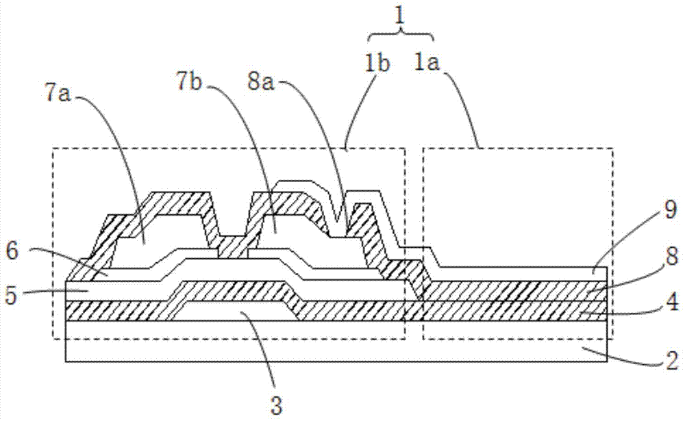
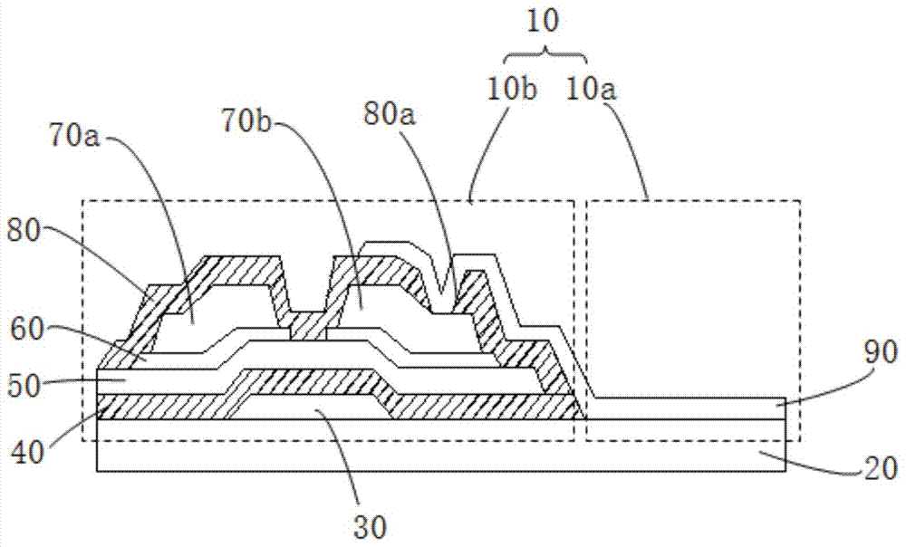
[0038] refer to figure 2 , an array substrate provided in this embodiment, which includes a glass substrate 20 and a plurality of pixel structures 10 formed on the glass substrate 20 (only a partial cross-section of one pixel structure 10 is shown in the drawings ), the pixel structure 10 includes a light-transmitting region 10a and a non-light-transmitting region 10b. Wherein, the non-transparent region 10 b includes a gate 30 , a gate insulating layer 40 , an active layer 50 , source / drain 70 ...


PUM


Abstract

The invention discloses an array substrate. The array substrate comprises a glass substrate and multiple pixel structures formed on the glass substrate, wherein each pixel structure comprises a transmitting area and a non-transmitting area, the non-transmitting area comprises a grid, a grid insulation layer, an active layer, a source/drain and a passivation layer which are sequentially formed on the glass substrate, the transmitting area comprises a pixel electrode directly formed on the glass substrate, and the pixel electrode extends to the non-transmitting area and is electrically connected with the source or the drain. The invention further discloses a preparation method of the array substrate as well as an LCD (liquid crystal display) panel comprising the array substrate.

Description

technical field [0001] The invention relates to the technical field of liquid crystal display, in particular to an array substrate and a preparation method thereof, and also to a liquid crystal panel including the array substrate. Background technique [0002] Liquid Crystal Display (LCD) is a flat and ultra-thin display device, and the liquid crystal panel is an important part of the liquid crystal display. A commonly used liquid crystal panel at least includes an array substrate and a color filter substrate oppositely arranged, and a liquid crystal layer located between the array substrate and the color filter substrate. [0003] The array substrate generally includes a glass substrate and a plurality of pixel structures formed on the glass substrate. figure 1 It is a structural schematic diagram of an existing array substrate, and only one pixel structure is shown in the figure as an example. Such as figure 1 As shown, the pixel structure 1 includes a light-transmittin...

Claims


Application Information

Patent Timeline
IPC IPC(8): H01L27/12G02F1/136G02F1/133
CPCH01L27/124G02F1/136227G02F1/133302G02F1/136295G02F1/133345G02F1/133514G02F1/134309G02F1/136286G02F1/1368G02F2201/123
Inventor 高冬子
Owner TCL CHINA STAR OPTOELECTRONICS TECH CO LTD
Why Eureka
Try Eureka