
Three-notch ultra-wideband filter based on defected microstrip structures

A technology of ultra-wideband filter and defect microstrip, which is applied in the direction of waveguide devices, circuits, electrical components, etc., can solve the problem of difficult adjustment of notch frequency band center frequency and bandwidth, unsatisfactory passband selectivity and stopband characteristics, and unfavorable Mass production and other issues, to achieve good in-band selection performance, good out-of-band suppression effect, and simple structure

Inactive Publication Date: 2015-07-22
NANJING UNIV OF SCI & TECH
View PDF5 Cites 3 Cited by
  • Summary
  • Abstract
  • Description
  • Claims
  • Application Information

AI Technical Summary

Problems solved by technology

[0007] In summary, the ultra-wideband filter with notch characteristics designed in Document 1 has a simple structure, but only one notch frequency band is obtained; the ultra-wideband filter with double notch characteristics designed in Document 2 is based on multiple layer circuit structure, but due to high production cost and imperfect technology, it is not conducive to mass production; the ultra-wideband filter with single-layer structure and three-notch characteristics designed in Document 3 is easy to process and integrate, but the selectivity of the passband And the stopband characteristics are not ideal, and the center frequency and bandwidth of the notch frequency band are not easy to adjust

Method used


Image

  • Three-notch ultra-wideband filter based on defected microstrip structures
  • Three-notch ultra-wideband filter based on defected microstrip structures
  • Three-notch ultra-wideband filter based on defected microstrip structures

Examples


Embodiment Construction

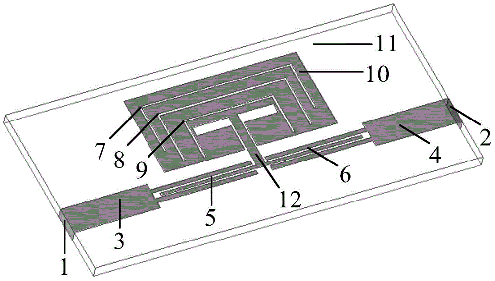
[0021] like figure 1 As shown, the three-notch ultra-wideband filter of the present invention includes a microstrip substrate 11, and the reverse side of the microstrip substrate 11 is used as a grounded metal plate of the three-notch ultra-wideband filter; two input channels are distributed on both sides of the microstrip substrate 11. Output ports, namely the first input\output port 1 and the second input\output port 2.

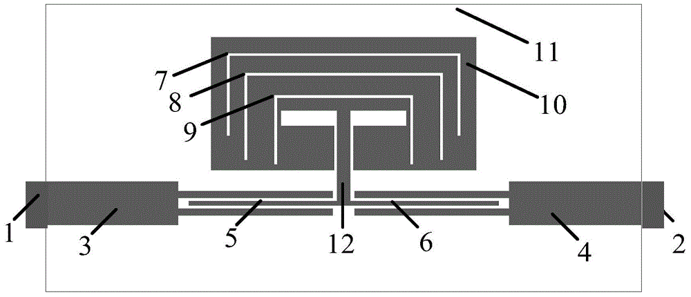
[0022] like figure 1 and figure 2 As shown, a first uniform line transmission unit 3 , a second uniform transmission line unit 4 , a first parallel coupled feeder 5 , a second parallel coupled feeder 6 , and an E-type multimode resonant structure 10 are arranged on the front surface of the microstrip substrate 11 .

[0023] The first uniform transmission line unit 3 and the second uniform transmission line unit 4 are respectively connected to the first input / output port 1 and the second input / output port 2, and the first uniform transmission line unit 3,...


PUM

PropertyMeasurementUnit
Thicknessaaaaaaaaaa

Abstract

The invention provides a three-notch ultra-wideband filter based on defected microstrip structures, which comprises a microstrip substrate, and a first input / output port, a second input / output port, a first uniform line transmission unit, a second uniform line transmission unit, a first parallel coupled feeder, a second parallel coupled feeder and an E-type multimode resonant structure arranged on the microstrip substrate, wherein a first defected microstrip structure, a second defected microstrip structure and a third defected microstrip structure are arranged on the E-type multimode resonant structure; and each defected microstrip structure is formed by three linear grooves connected in sequence and with the same width in the E-type multimode resonant structure. Three-notch features are provided, the central frequency of the notch is adjustable through adjusting the length of the defected microstrip structure, and product debugging and batch production are facilitated.

Description

technical field [0001] The invention belongs to the technical field of microwave transmission devices, and in particular relates to a triple-notch ultra-wideband filter based on a defect microstrip structure. Background technique [0002] Ultra-wideband (UWB) technology is an emerging wireless communication technology in the world due to its low cost, low power consumption, high data transmission rate, and good security in recent years. Since the US Federal Communications Commission (Federal Communications Commission, FCC) approved the frequency band of 3.1 GHz-10.6 GHz for commercial communication in 2002, UWB communication technology has received more and more attention. The filter is an important component in the UWB system. How to design a UWB bandpass filter with a compact structure and good performance has become a goal pursued by researchers. However, within the entire ultra-wideband frequency range, various other narrowband wireless communication signals already exi...

Claims


Application Information

Patent Timeline
IPC IPC(8): H01P1/203
Inventor 王建朋赵俊顶翁美丽何蓉蓉
Owner NANJING UNIV OF SCI & TECH
Learn More