Display panel, display device and manufacturing method

A display panel and display function technology, applied in optics, instruments, electrical digital data processing, etc., can solve the problems of low mass production yield, easy peeling, organic film damage, etc., and achieve the effect of improving product yield

Active Publication Date: 2015-07-29
XIAMEN TIANMA MICRO ELECTRONICS +1
View PDF10 Cites 45 Cited by
  • Summary
  • Abstract
  • Description
  • Claims
  • Application Information

AI Technical Summary

Problems solved by technology

[0004] In order to save the process flow, the existing in-cell touch screen generally reuses the common electrodes as touch electrodes, but the touch time will be compressed and occupy the display time, so the structure of time-division multiplexing of common electrodes and touch electrodes is difficult to adapt The development trend of high resolution and large size of display panel
However, in the traditional structure where the common electrodes and the touch electrodes are not reused, the touch electrodes are generally arranged on the side of the color filter substrate close to the liquid crystal layer. The bonding force of the electrodes is weak, and it is easy to peel off, and when etching the touch electrode pattern, it is easy to cause damage to the organic film layer of the color filter substrate, and the process compatibility is poor, so the mass production yield is low
In addition, since the color filter substrate side is used as the touch side, the distance between the touch position and the touch electrodes is relatively long, and the touch sensitivity is poor

Method used


Image

  • Display panel, display device and manufacturing method
  • Display panel, display device and manufacturing method
  • Display panel, display device and manufacturing method

Examples


Embodiment Construction

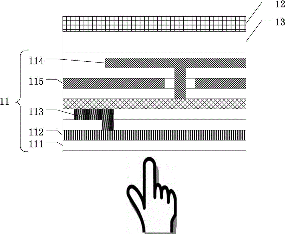
[0052] The present invention will be further described in detail below in conjunction with the accompanying drawings and embodiments. It should be understood that the specific embodiments described here are only used to explain the present invention, but not to limit the present invention. In addition, it should be noted that, for the convenience of description, only some structures related to the present invention are shown in the drawings but not all structures.

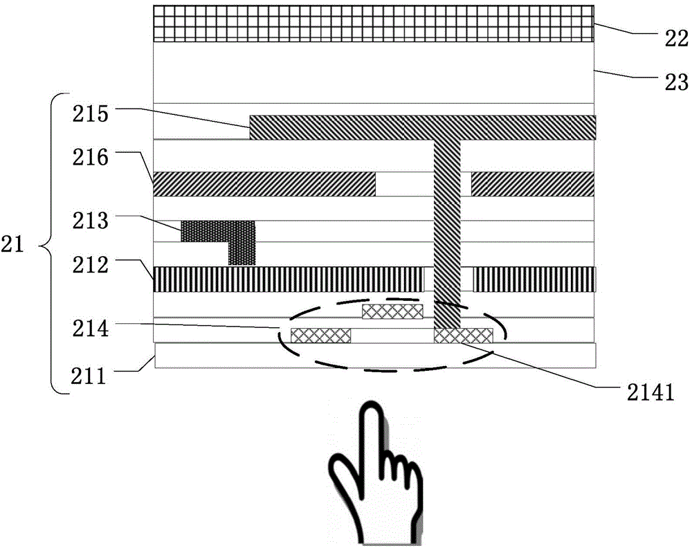
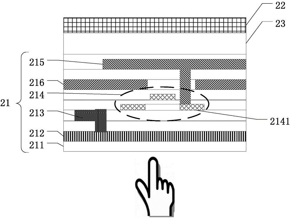
[0053] An embodiment of the present invention provides a display panel. figure 1 It is a schematic diagram of a partial cross-sectional structure of a display panel provided by an embodiment of the present invention. Such as figure 1As shown, the display panel includes: an array substrate 11, a color filter substrate 12 disposed opposite to the array substrate 11, and a display function layer 13 located between the array substrate 11 and the color filter substrate 12; wherein , the array substrate 11 includes a ...


PUM


Abstract

The invention discloses a display panel, a display device and a manufacturing method. The display panel comprises an array substrate, a color film substrate and a display function layer, wherein the color film substrate is opposite to the array substrate; the display function layer is positioned between the array substrate and the color film substrate; the array substrate comprises a substrate base plate, a plurality of touch electrode blocks, a plurality of touch signal lines, a pixel electrode and a public electrode; the touch electrode blocks are arranged on the side, adjacent to the display function layer, of the array substrate; each touch signal line corresponds to one touch electrode block; the pixel electrode and the public electrode are arranged above a touch electrode block film layer and are electrically insulated; the side, far away from the display function layer, of the array substrate is a touch side. The display device comprises the display panel, a backlight module and a driving chip, wherein the backlight module is positioned on the side, far away from the display function layer, of the color film substrate of the display panel; the driving chip is used for a display driver and a touch driver. The compatibility, the product yield and the touch sensitivity of a preparation process are improved.

Description

technical field [0001] The embodiments of the present invention relate to the technical field of touch display, and in particular, to a display panel, a display device and a manufacturing method. Background technique [0002] With the development of electronic technology, the functions of display devices are not limited to receiving video signals and displaying them. Today's display devices are also integrated with touch functions, that is, they can input control information according to the operator's touch operation information on the display device. instruction. [0003] Currently, the display devices with touch function can be divided into three types according to the structure: an external touch screen, a surface-covered touch screen, and a built-in touch screen. Among them, the embedded touch screen embeds the touch electrodes of the touch screen inside the liquid crystal display, which can reduce the overall thickness of the module and greatly reduce the production c...

Claims


Application Information

Patent Timeline
Patent Type & Authority Applications(China)
IPC IPC(8): G02F1/1333G02F1/1343G02F1/1362G06F3/041
CPCG02F1/13338G02F1/134309G02F1/1362G02F1/136286G02F1/1368G06F3/041G06F3/0412
Inventor 文亮
Owner XIAMEN TIANMA MICRO ELECTRONICS
Why Eureka
Try Eureka