

Digital image processing method and digital image processing device
A technology of digital images and processing methods, applied in the computer field, can solve the problems of skin texture differences, inability to display processing effects in real time, and inability to realize automatic processing, and achieve the effect of inconspicuous traces
- Summary
- Abstract
- Description
- Claims
- Application Information
AI Technical Summary
Problems solved by technology
Method used
Image

Examples
Embodiment 1
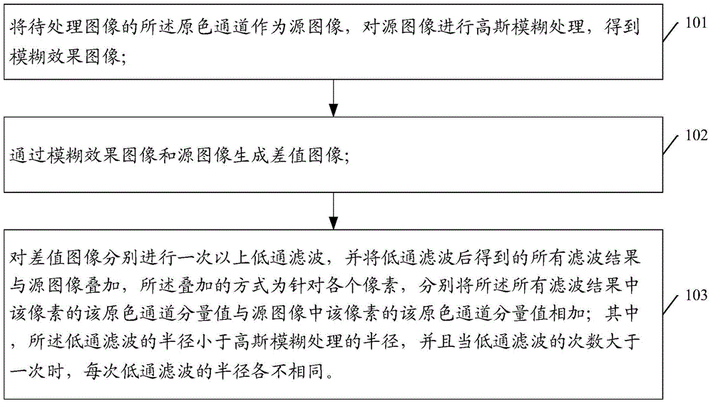
[0051] In this embodiment, the processing of the R channel of the digital image is taken as an example for description, and the manner of processing the G channel and the B channel of the digital image is the same. In this embodiment, the dark circle and its surrounding area in the face image are taken as the image to be processed.
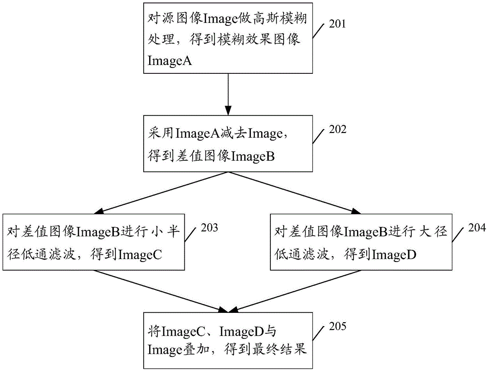
[0052] Such as figure 2 As shown, the R channel of the image to be processed is used as the source image (denoted as Image), and the following steps are performed for the source image Image:
[0053]Step 201: Perform Gaussian blur processing with a large radius on the source image Image to obtain a blurred image (denoted as ImageA). The radius of Gaussian blur processing here is generally 10 to 16 pixels
[0054] After processing in this step, the display effect of the blurred image ImageA is: the R value of the pixel whose original R value is larger than the surrounding area will become smaller, and the R value of the pixel whose original R va...
Embodiment 2
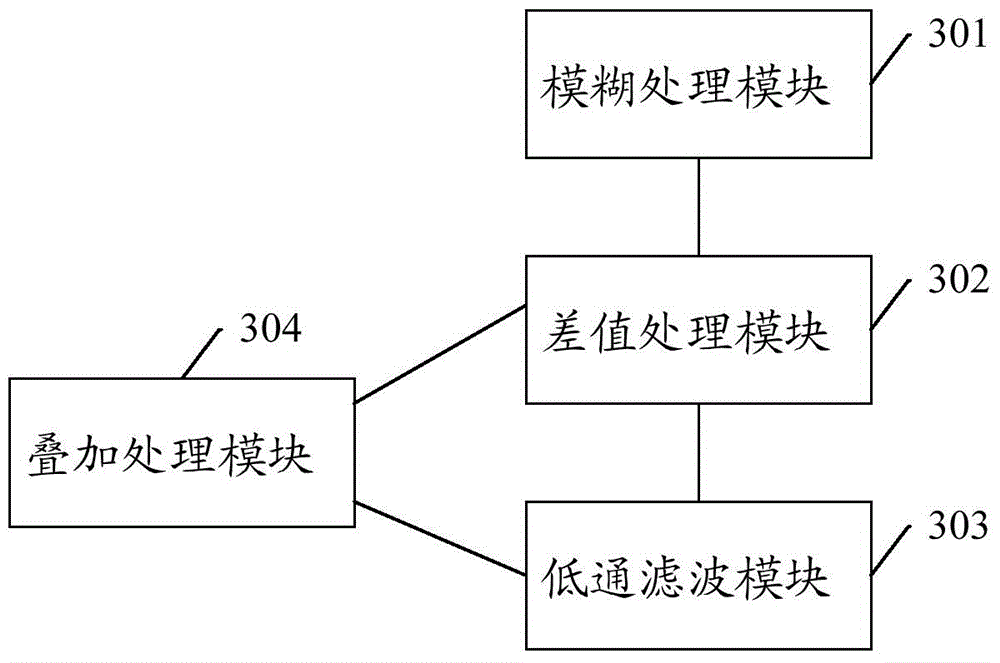
[0082] This embodiment introduces a specific digital image processing device, such as Figure 4 It is a schematic diagram of the structure of the device, including:
[0083] At least one processor 401 , at least one memory 402 , at least one network interface 403 , at least one input device 404 (such as a mouse, keyboard, etc.), at least one output device 405 (such as a display screen), and at least one communication bus 406 .
[0084] Wherein, the network interface 403 may include a standard wired interface, a wireless interface (such as a WI-FI interface), and the like.
[0085] The communication bus 406 is used to implement connection communication between these components.
[0086] The memory 402 may be a high-speed RAM memory, or a non-volatile memory (non-volatile memory), such as at least one disk memory. Optionally, the memory 402 may also be at least one storage device located far away from the aforementioned processor 401 . Such as Figure 4 As shown, the memory ...
PUM
 Abstract
Description
Claims
Application Information