Image sensor

A technology of image sensor and photosensitive area, applied in the field of image sensor, can solve the problem that the performance of image sensor needs to be improved, etc.

Active Publication Date: 2015-07-29
CHINA WAFER LEVEL CSP
View PDF5 Cites 4 Cited by
  • Summary
  • Abstract
  • Description
  • Claims
  • Application Information

AI Technical Summary

Problems solved by technology

[0006] However, the performance of existin

Method used


Image

  • Image sensor
  • Image sensor
  • Image sensor

Examples


Embodiment Construction

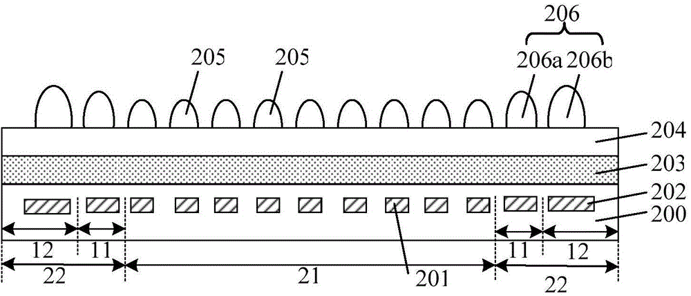
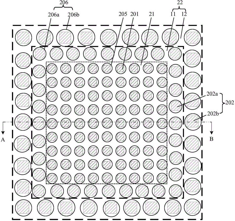
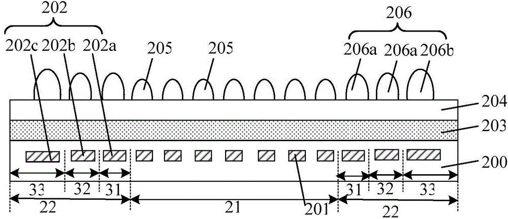
[0028] As mentioned in the background art, the performance of existing image sensors still needs to be improved. For example, existing image sensors still have problems such as easy distortion and deformation of edge imaging.

[0029] The study found that in the microlens design, all microlenses have the same width and height, so the response characteristics of each microlens to light are also the same, but in actual use, due to the influence of factors such as the package frame, the edge The incident light received by the microlenses is less than that received by the central microlens, so the image at the edge of the photosensitive area of ​​the image is easily distorted and deformed, and the closer to the edge area, the more serious the distortion and deformation of the image at the photosensitive area.

[0030] For this reason, the present invention provides an image sensor, the size of the microlens in the edge area is larger than the size of the microlens in the middle are...


PUM


Abstract

An image sensor comprises a semiconductor substrate, comprising a middle region and an edge region surrounding the middle region, and a micro lens. The middle region of the semiconductor substrate is provided with multiple first photosensitive regions, the edge region of the semiconductor substrate is provided with multiple second photosensitive regions, and the size of the second photosensitive regions of the edge region is smaller than that of the first photosensitive regions of the middle regions; the micro lens is located on the semiconductor substrate and includes multiple first micro lenses located in the middle region of the semiconductor substrate and multiple second micro lenses located in the edge region of the semiconductor substrate, the first micro lenses are located above the corresponded first photosensitive regions, the second micro lenses are located above the corresponded second photosensitive regions, and the size of the second micro lenses of the edge region of the semiconductor substrate is larger than that of the first micro lenses of the middle region of the semiconductor substrate. By the aid of the image sensor, the imaging quality of the edge region is improved.

Description

technical field [0001] The invention relates to the field of image sensors, in particular to an image sensor for optimized imaging. Background technique [0002] With the rapid development of electrical technology and electronic technology, more and more modern mobile electronic products using image sensor technology, such as smart phones, digital cameras, notebook computers, etc., have been rapidly developed and popularized. At present, people spend more and more on mobile phones and other electronic products, and their requirements for product quality and personal experience are becoming more and more stringent. Electronic products now have camera and video functions, and the number of pixels has grown from hundreds of thousands to 5 million, 8 million or even higher. As the main component of electronic product imaging, the image sensor has higher and higher requirements for its imaging quality. [0003] An image sensor is a device that converts light signals into electr...

Claims


Application Information

Patent Timeline
IPC IPC(8): H01L27/146
Inventor 王之奇喻琼王蔚
Owner CHINA WAFER LEVEL CSP
Why Eureka
Try Eureka