Array substrate, preparation method thereof, display panel and display device

A technology of array substrate and insulating layer, applied in semiconductor/solid-state device manufacturing, instruments, semiconductor devices, etc., can solve the problem of easy color mixing, and achieve the effect of reducing influence, improving liquid crystal efficiency, and reducing driving voltage

Inactive Publication Date: 2015-08-12
BOE TECH GRP CO LTD
View PDF6 Cites 7 Cited by
  • Summary
  • Abstract
  • Description
  • Claims
  • Application Information

AI Technical Summary

Problems solved by technology

Under this structure, the common electrode is a structure without slits. Because of the interference of the electric field of the adjacent pixels under the structure without slits, color mixing is prone to occur.

Method used


Image

  • Array substrate, preparation method thereof, display panel and display device
  • Array substrate, preparation method thereof, display panel and display device
  • Array substrate, preparation method thereof, display panel and display device

Examples


Embodiment Construction

[0035] In order to avoid the problem of color mixing caused by mutual influence of adjacent pixels, the embodiments of the present invention provide an array substrate, a manufacturing method thereof, a display panel and a display device.

[0036] The preferred embodiments of the present invention will be described below in conjunction with the accompanying drawings. It should be understood that the preferred embodiments described here are only used to illustrate and explain the present invention, and are not intended to limit the present invention, and in the absence of conflict, the present invention The embodiments and the features in the embodiments can be combined with each other.

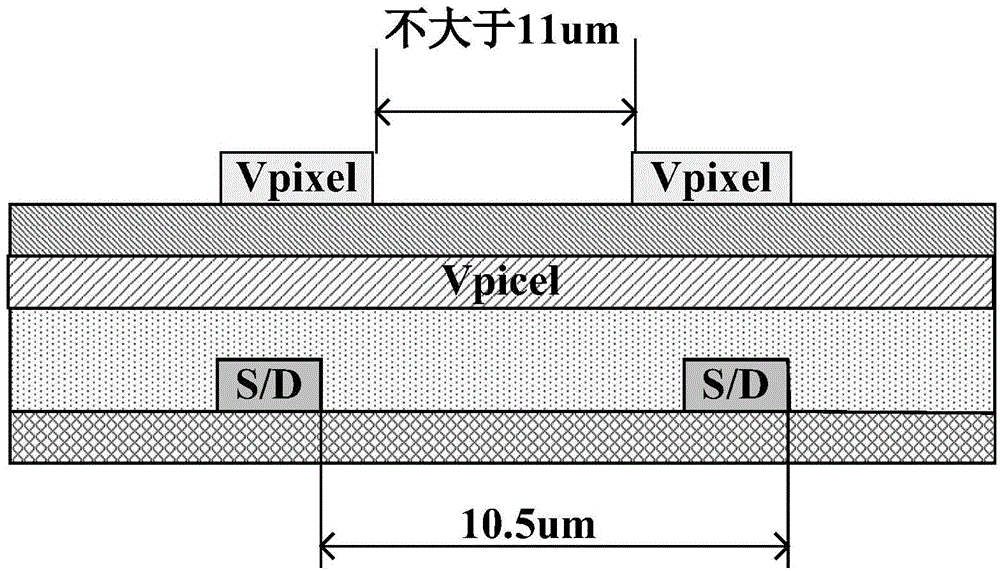
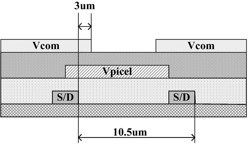
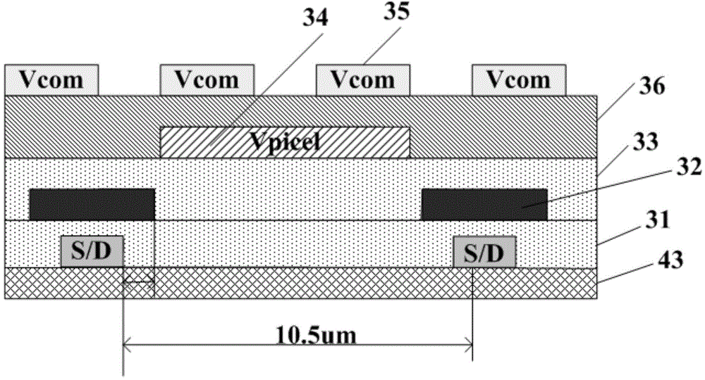
[0037] The array substrate provided by the embodiment of the present invention includes a plurality of gate lines and a plurality of data lines intersecting, and a plurality of intersecting gate lines and a plurality of data lines define a plurality of pixel regions, and each pixel region inclu...


PUM


Abstract

The invention discloses an array substrate, a preparation method thereof, a display panel and a display device. At least two public electrode slots are formed. The problem that adjacent pixels are affected to cause color mixing is avoided, and meanwhile the liquid crystal efficiency is improved. The array substrate comprises a plurality of grid lines and a plurality of data lines which are crossed. A plurality of pixel areas are defined by the crossed grid lines and data lines. Each pixel area comprises a thin film transistor and further comprises a first insulation layer, a metal layer, a second insulation layer, a pixel electrode and a public electrode, wherein the first insulation layer is arranged above the thin film transistor and the corresponding data line, the metal layer is arranged above the first insulation layer, the second insulation layer is arranged above the metal layer, the pixel electrode and the public electrode are arranged above the second insulation layer, and a third insulation layer is arranged between the pixel electrode and the public electrode. The public electrode in each pixel area at least comprises two slots. The metal layers cover the data lines.

Description

technical field [0001] The present invention relates to the technical field of liquid crystal display, in particular to an array substrate and a preparation method thereof, a display panel and a display device. Background technique [0002] With the development of liquid crystal display technology, flat panel displays have replaced CRT (Cathode Ray Tube, cathode ray tube) displays to become mainstream products in the display field. Currently, common flat panel displays include LCD (Liquid Crystal Display, liquid crystal display) and OLED (Organic Light-Emitting Diode, organic light-emitting diode) displays. During the imaging process, each liquid crystal pixel in the LCD display is integrated in a TFT (Thin Film Transistor, Thin Film Transistor) to drive, and cooperate with the peripheral driving circuit to realize image display. [0003] In the ADS (ADvanced Super Dimension Switch, advanced ultra-dimensional field switching technology) mode, two layers of transparent elect...

Claims


Application Information

Patent Timeline
Patent Type & Authority Applications(China)
IPC IPC(8): G02F1/1362G02F1/1343H01L27/12H01L21/77
CPCG02F1/134309G02F1/136227G02F1/136286H01L27/1214H01L27/1259G02F1/1362G02F1/136218G02F1/134372G02F1/136295G02F1/133345G02F1/133514G02F1/13439G02F1/1368G02F2201/121G02F2201/123H01L27/1222H01L27/124H01L27/1248H01L27/1262H01L29/66765H01L29/78669
Inventor 崔贤植
Owner BOE TECH GRP CO LTD
Why Eureka
Try Eureka