Pixel structure, array substrate and display device
A pixel structure and sub-pixel technology, applied in the field of array substrates, display devices, and pixel structures, can solve problems such as affecting the transmittance of liquid crystal displays, and achieve the effects of improving chromatic aberration, reducing influence and brightness difference.
- Summary
- Abstract
- Description
- Claims
- Application Information
AI Technical Summary
Problems solved by technology
Method used
Image


Examples
Embodiment 1
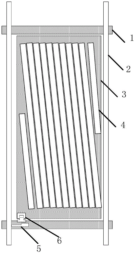
[0048] This embodiment provides a pixel structure, including a plurality of sub-pixel units driven by the same gate line and the same data line, wherein each of the sub-pixel units is composed of more than two sub-pixels, each of which The sub-pixel unit is divided into N display areas, and in the electrified state, the electric field generated by each display area is different so that the sub-pixel unit realizes N-domain display.
[0049] In this embodiment, the sub-pixel units driven by the same gate line and the same data line are divided into multiple display areas. In the energized state, the electric fields generated by each display area are different. The deflection angles of the liquid crystals in different regions are different, and multi-domain display can be realized, so that the brightness difference of the liquid crystal display device adopting the pixel structure is further reduced, and the chromatic aberration phenomenon is effectively improved. In addition, sin...
Embodiment approach 1
[0055] Embodiment 1: the inclination angles of the striped pixel electrodes in the first region S1 and the third region S3 are the same, and similarly, the inclination angles of the striped pixel electrodes in the second region S2 and the fourth region S4 are the same, and the first thin film transistor and the The channel width-to-length ratio of the second thin film transistor is the same, the areas of the first region S1 and the third region S3 are different, and the areas of the second region S2 and the fourth region S4 are different, so that in the electrified state, each display region The deflection angles of liquid crystals are different, and the liquid crystal 7 in the liquid crystal display device has four kinds of deflection angles, such as Figure 9 As shown, therefore, the anisotropy of the liquid crystal is well averaged under different viewing angles, and the chromatic aberration of the liquid crystal display device can be further reduced. Among them, in order t...
Embodiment approach 2
[0056] Embodiment 2: the inclination angles of the striped pixel electrodes in the first region S1 and the third region S3 are the same, and similarly, the inclination angles of the striped pixel electrodes in the second region S2 and the fourth region S4 are the same, and the first thin film transistor and the The channel width-to-length ratios of the second thin film transistors are different, the areas of the first region S1 and the third region S3 are the same, and the areas of the second region S2 and the fourth region S4 are the same, so that in the electrified state, each display region The deflection angles of liquid crystals are different, and the liquid crystal 7 in the liquid crystal display device has four kinds of deflection angles, such as Figure 9 As shown, therefore, the anisotropy of the liquid crystal is well averaged under different viewing angles, and the chromatic aberration of the liquid crystal display device can be further reduced.
PUM
 Abstract
Description
Claims
Application Information
 - R&D
- Intellectual Property
- Life Sciences
- Materials
- Tech Scout
- Unparalleled Data Quality
- Higher Quality Content
- 60% Fewer Hallucinations
Browse by: Latest US Patents, China's latest patents, Technical Efficacy Thesaurus, Application Domain, Technology Topic, Popular Technical Reports.
© 2025 PatSnap. All rights reserved.Legal|Privacy policy|Modern Slavery Act Transparency Statement|Sitemap|About US| Contact US: help@patsnap.com