LED material strap manufacturing method

A technology for a light-emitting diode and a manufacturing method, which is applied to semiconductor devices, electrical components, circuits, etc., can solve the problems of assembly fees, time and labor, and achieve the effect of simplifying the manufacturing method and subsequent processes.

Inactive Publication Date: 2015-08-12
I CHIUN PRECISION ELECTRIC IND CHINA
View PDF6 Cites 4 Cited by
  • Summary
  • Abstract
  • Description
  • Claims
  • Application Information

AI Technical Summary

Problems solved by technology

Therefore, in the conventional technology, although the light-emitting diode die can be packaged in a tape type to speed up the packaging process, the assembly procedure after packaging is still quite time-consuming and labor-intensive.

Method used


Image

  • LED material strap manufacturing method
  • LED material strap manufacturing method
  • LED material strap manufacturing method

Examples


Embodiment Construction

[0032] refer to figure 1 , the invention provides a method for manufacturing a light-emitting diode strip, the method at least comprising figure 1 Steps a-d shown in . The manufacturing method of the light-emitting diode strip provided in the first embodiment of the present invention preferably includes the following steps:

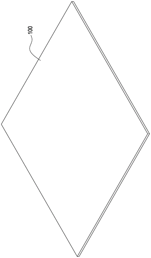
[0033] refer to figure 1 and figure 2 , In step a, a metal substrate 100 is provided, and the metal substrate is preferably a strip-shaped metal sheet.

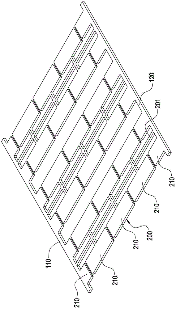
[0034] refer to figure 1 and image 3 In step b, the metal substrate 100 is cut to form the connection frame 110 / 120 and the carrier sheet 200 . In this embodiment, the metal substrate 100 is preferably stamped and cut with a knife, and the two longitudinal sides of the metal substrate 100 are cut to form two elongated connection frames 110 / 120 arranged in parallel and spaced apart. Each carrier sheet 200 is elongated and its two ends are respectively connected to one of the connection frames...


PUM


Abstract

Provided is an LED material strap manufacturing method, including the steps of: providing a metal substrate; cutting the metal substrate to form a connection framework and a plurality of bearing sheets, wherein one end of each bearing sheet is in connection with the connection framework, and each bearing sheet includes a plurality of conductive segments arranged at intervals; an insulation segment formed between any two adjacent conductive segments so as to connect the two conductive segments; and a plurality of insulation frames arranged at intervals on each bearing sheet, wherein each insulation frame corresponds with the position of one of the insulation segments to enclose a recess on the upper surface of each carrying sheet, and each insulation segment and two conductive segments connected by insulation segments are exposed in corresponding recesses.

Description

technical field [0001] The invention relates to the technical field of light-emitting diode material strips, in particular to a manufacturing method of light-emitting diode material strips. Background technique [0002] The structure of the conventional light-emitting diode strip is that the light-emitting diode crystal grains are arranged on the strip and packaged, and the light-emitting diode crystal grains on the strip are insulated from each other. Before it is used, it is necessary to cut the sealed light-emitting diode crystal grains from the material tape, and then assemble them according to different usage requirements. Therefore, in the prior art, although the light-emitting diode chips can be packaged in a tape type to speed up the packaging process, the assembly procedure after packaging is still quite time-consuming and labor-intensive. [0003] In view of this, the inventor of the present invention has focused on the above-mentioned prior art, and combined with...

Claims


Application Information

Patent Timeline
Patent Type & Authority Applications(China)
IPC IPC(8): H01L33/00H01L33/62
Inventor 林佑任李廷玺
Owner I CHIUN PRECISION ELECTRIC IND CHINA
Why Eureka
Try Eureka