Crystal-covering package method and structure for covering crystal

A technology of flip-chip packaging and flip-chip, which is applied in semiconductor/solid-state device manufacturing, electrical components, electric solid-state devices, etc., and can solve problems such as limiting the application range of flip-chip packaging, high cost, and complexity

Inactive Publication Date: 2005-10-05
LINGSEN PRECISION INDS
View PDF0 Cites 0 Cited by
  • Summary
  • Abstract
  • Description
  • Claims
  • Application Information

AI Technical Summary

Problems solved by technology

[0003] In the prior art, in order to solder the chip on the lead frame, it is necessary to form a flip-chip solder bump on the die surface of the chip. The dielectric layer electrically connected to the lead frame; however, generally the dielectric layer needs to be fabricated o

Method used


Image

  • Crystal-covering package method and structure for covering crystal
  • Crystal-covering package method and structure for covering crystal
  • Crystal-covering package method and structure for covering crystal

Examples


Embodiment Construction

[0017] In order to have a more in-depth understanding and recognition of the features, purposes, and effects of the present invention, the preferred embodiments are listed as follows with accompanying drawings:

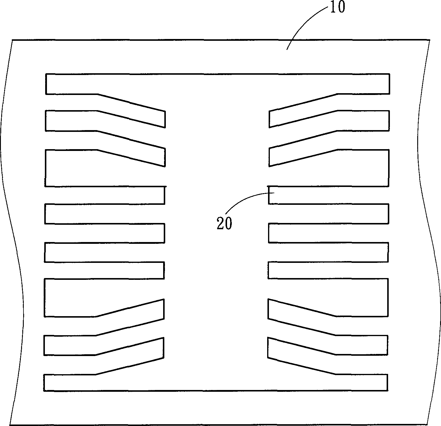
[0018] See figure 1 , Is a lead frame 10 made by etching, which has a plurality of flip-chip regions 20, which are used to connect with the die pads 70 of the wafer 80 (see Figure 5 ).

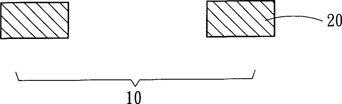
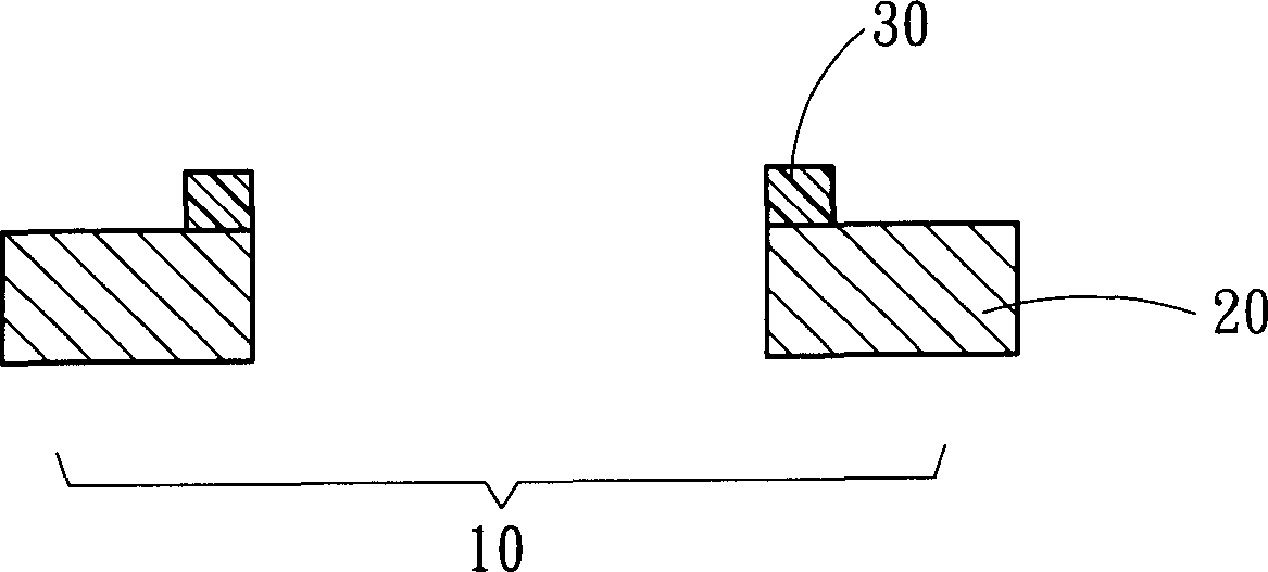
[0019] See picture 2-1 , Figure 2-2 , Figure 2-3 ,versus Figure 2-4 , Is a schematic diagram of the half-etching process, a lead frame 10 with multiple flip-chip regions 20, such as picture 2-1 Shown; use the method of exposure and development to form a photoresist layer 30 on a specific area of ​​the flip chip area 20, such as Figure 2-2 As shown; using the etching solution again, the flip chip area 20 has not covered the photoresist layer 30 area contact with the etching solution for etching, and the etching time is controlled, so that the flip chip area 20 is formed with flip c...


PUM


Abstract

Using semi-etching method etches out composite crystal soldered blocks in time of preparing conducting wire holder. Gold, silver, or soldering tin etc. metals are plated on composite crystal soldered blocks. Soldering pads of chip on wafer are connected to composite crystal soldered blocks so as to form conducting connection. Finally, filling packing material forms encapsulation. The method does not need to develop composite crystal soldered blocks on soldering pads of chip, and the original equipment for preparing conducting wire holder is available. Thus, the invention simplifies manufacturing procedure and lowers cost.

Description

Technical field [0001] The present invention relates to flip chip packaging, in particular to a flip chip packaging method using a lead frame and a flip chip structure. Background technique [0002] Flip Chip (Flip Chip) packaging is an advanced semiconductor packaging technology. Compared with the general traditional Ball Grid Array (BGA) semiconductor packaging technology, the biggest difference is that the structure of flip chip packaging is The bonding pad surface is mounted on the lead frame (substrate) in an upside-down manner, and then soldered to it with multiple flip chip bumps to electrically connect the chip to the lead frame, because the flip chip package does not need to be used The space-consuming bonding wires provide electrical connections between the chip and the lead frame, so the overall size of the packaged product can be effectively reduced. [0003] In the prior art, to solder the chip on the lead frame, it is necessary to form flip chip solder bumps on the ...

Claims


Application Information

Patent Timeline
IPC IPC(8): H01L21/56H01L21/60H01L23/495
CPCH01L2224/16245
Inventor 何秀芬杜明德
Owner LINGSEN PRECISION INDS
Why Eureka
Try Eureka