
A kind of array substrate and manufacturing method thereof

An array substrate and substrate technology, which is applied in the field of flat panel display, can solve the problem of poor viewing angle in the oblique direction, and achieve the effect of improving the effect of wide viewing angle and good visual effect.

Active Publication Date: 2019-02-12
SHENZHEN LAIBAO HI TECH
View PDF6 Cites 0 Cited by
  • Summary
  • Abstract
  • Description
  • Claims
  • Application Information

AI Technical Summary

Problems solved by technology

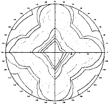
[0004] like Figure 4 shown, which is figure 1 The contrast viewing angle curve of the AIFF MVA liquid crystal cell in the middle, it can be seen from the figure that although the viewing angles in the horizontal and vertical directions are better, the viewing angles in the oblique directions (30°-60°, 120°-150°, 210°-240° ° and 300°-330°) are relatively poor

Method used


Image

  • A kind of array substrate and manufacturing method thereof
  • A kind of array substrate and manufacturing method thereof
  • A kind of array substrate and manufacturing method thereof

Examples


Embodiment Construction

[0036] In order to illustrate the array substrate provided by the present invention and the manufacturing method thereof, the detailed description will be described below in conjunction with the accompanying drawings and text descriptions of the specification.

[0037] Please refer to Figure 5 , is a schematic structural view of an array substrate 200 according to a preferred embodiment of the present invention. The array substrate 200 can be a substrate in AIFF MVA mode, or an array substrate in other modes, and it at least includes a first surface 201a of the substrate 201, the first surface 201a is a continuous and smooth plane, in its embodiment, the first surface can be a curved surface or with an irregular surface, the substrate 201 is a transparent material such as hard Made of glass, rigid or flexible resin.

[0038]The array substrate 200 further includes a plurality of scanning lines 206 and a plurality of signal lines 205 formed on the first surface 201a of the su...


PUM


Abstract

The invention discloses an array substrate and a manufacturing method for the same. The array substrate at least comprises a substrate having a first surface. A plurality of pixel areas are formed on the first surface; a pixel electrode is formed in each pixel area; each pixel electrode comprises at least one first area, a second area and a third area; the first area is electrically connected with the third area via the second area; and a projection area of the first and third areas on the first surface is larger than a projection area of the second area on the first area.

Description

technical field [0001] The present invention relates to the field of flat panel display technology, in particular to an array substrate and a manufacturing method thereof. Background technique [0002] At present, the display modes of TFT-LCD (Thin Film Transistor Liquid Crystal Display) mainly include TN (Twisted Nematic, twisted nematic) mode, VA (Vertical Alignment, vertical alignment) mode, IPS (In-Plane-Switching , planar direction switching) mode, ADS (Advanced Super Dimension Switch, hyper-dimensional field switching) mode, MVA (Muti-domain Vertical Alignment, multi-domain vertical alignment) mode and AIFF MVA (Amiplified Intrinsic Fringe Field Controlled Muti-domain Vertical Alignment, strengthened liquid crystal Inner edge electric field effect multi-domain vertical orientation) and other modes. [0003] like figure 1 , figure 2 and image 3 Shown is a schematic diagram of the structure of an AIFF MVA liquid crystal cell, a schematic diagram of the working prin...

Claims


Application Information

Patent Timeline
Patent Type & Authority Patents(China)
IPC IPC(8): G02F1/1362G02F1/1368G02F1/1343
CPCG02F1/134309G02F1/134363G02F1/1368
Inventor 王士敏谢凡赵约瑟张超徐爽刘立峰李绍宗
Owner SHENZHEN LAIBAO HI TECH
Learn More