DDR frequency conversion design method and device
A technology of a frequency conversion device and a design method, applied in the field of data communication, can solve the problems of cumbersome steps, high hardware cost, complicated operation and the like
- Summary
- Abstract
- Description
- Claims
- Application Information
AI Technical Summary
Problems solved by technology
Method used
Image
Examples
Embodiment Construction
[0043] In order to explain in detail the technical content, structural features, achieved goals and effects of the technical solution, the following will be described in detail in conjunction with specific embodiments and accompanying drawings.
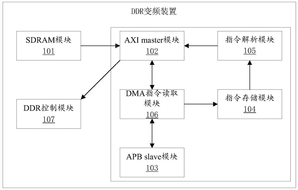
[0044] see figure 1, is a schematic diagram of a DDR frequency conversion device according to an embodiment of the present invention. The device includes an SDRAM module 101, an AXI master module 102, an APB slave module 103, an instruction storage module 104, an instruction analysis module 105, and a DMA instruction reading module 106; the SDRAM module is connected with the AXI master102 module, and the AXI master102 module Connect with instruction analysis module 105, described instruction analysis module 105 is connected with instruction storage module 104, and described instruction storage module 104 is connected with DMA instruction reading module 106, and described DMA instruction reading module 106 is connected with AXI master ...
PUM
 Abstract
Description
Claims
Application Information


