A method of making vdmos

A manufacturing method and conductive type technology, applied in the field of VDMOS manufacturing method and a VDMOS device, can solve the problems of cumbersome device manufacturing process, high cost, large gate-drain capacitance, etc., save photolithography and etching steps, and increase local thickness , Reduce the effect of gate-drain capacitance

Active Publication Date: 2018-03-30
FOUNDER MICROELECTRONICS INT
View PDF6 Cites 0 Cited by
  • Summary
  • Abstract
  • Description
  • Claims
  • Application Information

AI Technical Summary

Problems solved by technology

[0005] The invention provides a VDMOS manufacturing method and a VDMOS device to solve the technical problems of cumbersome device manufacturing process, high cost and large gate-drain capacitance in the prior art

Method used


Image

  • A method of making vdmos
  • A method of making vdmos
  • A method of making vdmos

Examples


Embodiment 1

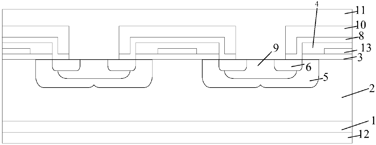
[0073] The following takes the whole process of growing a VDMOS device as an example to describe the implementation method of the embodiment of the present invention in detail, see Figure 8 :

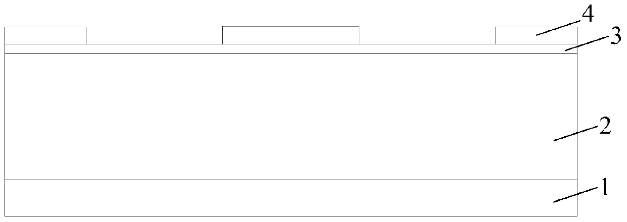
[0074] Step 801: Form a thick oxide layer on the epitaxial layer.

[0075] Figure 9 Among them, 1 is the N-type substrate, and 2 is the N-type epitaxial layer. In this step, at 900-1200°C, a plurality of block-shaped discrete thick oxide layers with a thickness of 0.5-2.0 μm are formed on the N-type epitaxial layer 2 13.

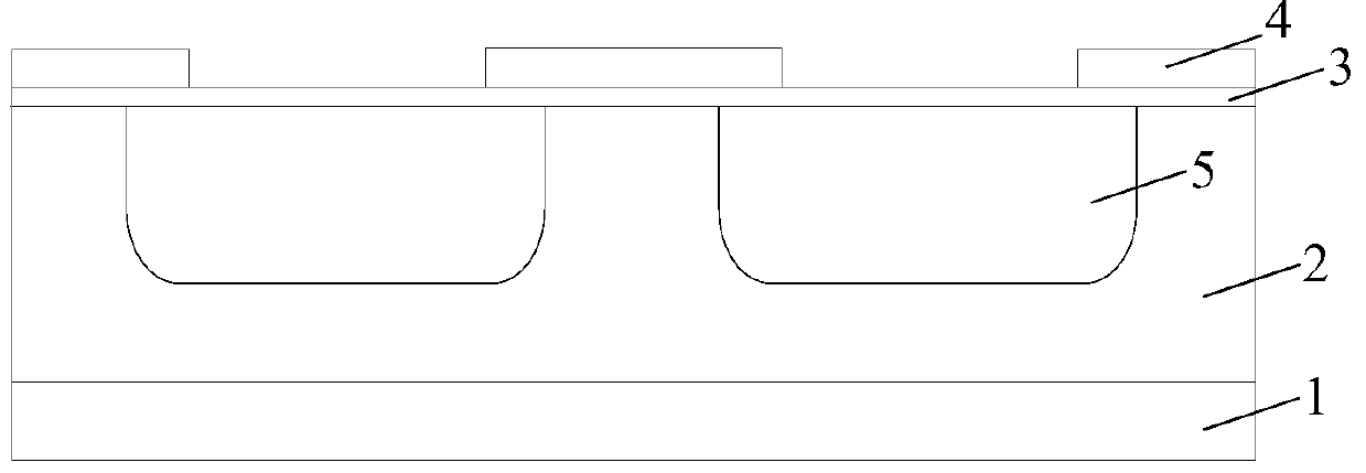
[0076] Step 802 : forming a gate oxide layer 3 .

[0077] In this step, the gate oxide layer 3 is formed between the N-type epitaxial layer 2 and the thick oxide layer 13. The growth temperature of the gate oxide layer is 900-1100° C., and the thickness is 0.05-0.20 μm. Oxygen, which oxidizes the interface, see Figure 10 .

[0078] Step 803: Fabricate polysilicon 4.

[0079] In this step, the growth temperature of the polysilicon 4 is 500-700° C., and the th...


PUM


Abstract

The present invention provides a VDMOS fabrication method and a VDMOS device, comprising: fabricating a plurality of bulky and discrete thick oxide layers on the epitaxial layer; fabricating a gate oxide layer between the epitaxial layer and the thick oxide layer; growing Gate, each gate covers the thick oxide layer area and the area where only the gate oxide layer exists, and there is a block-shaped discrete thick oxide layer between each adjacent two gates; between two adjacent gates Forming a continuous body region whose edge does not overlap with the thick oxide layer area covered by the gate; implanting ions of the first conductivity type to form a source separated by a thick oxide layer between two adjacent gates region; etch and remove the thick oxide layer between two adjacent gates; grow a silicon nitride layer, implant heavily doped ions of the second conductivity type, and make a dielectric layer, contact holes, front metal layer and back metal Floor. The invention optimizes the manufacturing process, reduces the manufacturing cost, and reduces the grid-drain capacitance.

Description

technical field [0001] The invention relates to the technical field of semiconductor manufacturing technology, in particular to a VDMOS manufacturing method and a VDMOS device. Background technique [0002] For an example of the fabrication method of an existing planar VDMOS device, see Figure 1 to Figure 6 : first form a gate oxide layer on the substrate and epitaxial layer and make a polysilicon gate, see figure 1 , wherein 1 is an N-type substrate, 2 is an N-type epitaxial layer, 3 is a gate oxide layer, and 4 is polysilicon; then implantation and driving into the P-body region 5 are performed, see figure 2 ; Carry out photolithographic etching on the gate oxide layer 3 surface again, and form N+ source region 6, see image 3 , wherein 7 is a photoresist; then a silicon nitride layer 8 is grown to drive in the P+ region 9, see Figure 4 ; On this basis, continue to grow the dielectric layer 10 to form a contact hole, see Figure 5 ; Finally, the front metal layer 11...

Claims


Application Information

Patent Timeline
Patent Type & Authority Patents(China)
IPC IPC(8): H01L21/336H01L29/78H01L29/423
Inventor 马万里
Owner FOUNDER MICROELECTRONICS INT
Why Eureka
Try Eureka