Supercharge Your Innovation With Domain-Expert AI Agents!

Array substrate structure and production method thereof

A technology of an array substrate structure and a manufacturing method, which is applied in semiconductor/solid-state device manufacturing, instruments, semiconductor devices, etc., can solve the problems of reduced light transmittance of the common electrode 910, poor light transmittance, and influence on the display effect of the panel, so as to improve the display effect, effect reduction, high transmittance effect

Active Publication Date: 2015-08-26
SHENZHEN CHINA STAR OPTOELECTRONICS TECH CO LTD +1
View PDF5 Cites 7 Cited by
  • Summary
  • Abstract
  • Description
  • Claims
  • Application Information

AI Technical Summary

Problems solved by technology

[0010] i.e. the SiH 4 , NH 3 , and N 2 React to form SiN under the action of electromagnetic field generated by RF power (radio frequency power) x :H and H 2 , the H produced by the reaction 2 The atmosphere is reducing, and it is easy to reduce the surface area of ​​the common electrode 910, such as figure 2 As shown, a reduced ITO layer 912 is formed on the surface of the common electrode 910. Below the reduced ITO layer 912 is an ITO layer 914. Due to the poor light transmittance of the reduced ITO layer 912, the overall common electrode 910 The light transmittance is greatly reduced, which in turn reduces the overall light transmittance of the touch display panel, which affects the display effect of the panel (such as brightness, etc.)

Method used


Image

  • Array substrate structure and production method thereof
  • Array substrate structure and production method thereof
  • Array substrate structure and production method thereof

Examples


Embodiment Construction

[0057] In order to further illustrate the technical means adopted by the present invention and its effects, the following describes in detail in conjunction with preferred embodiments of the present invention and accompanying drawings.

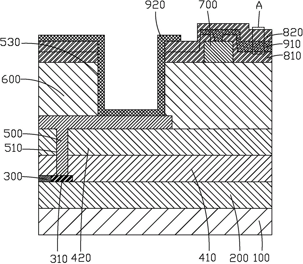
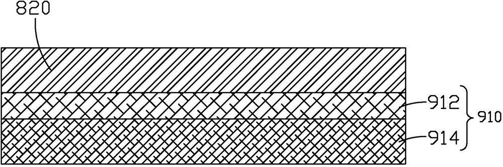
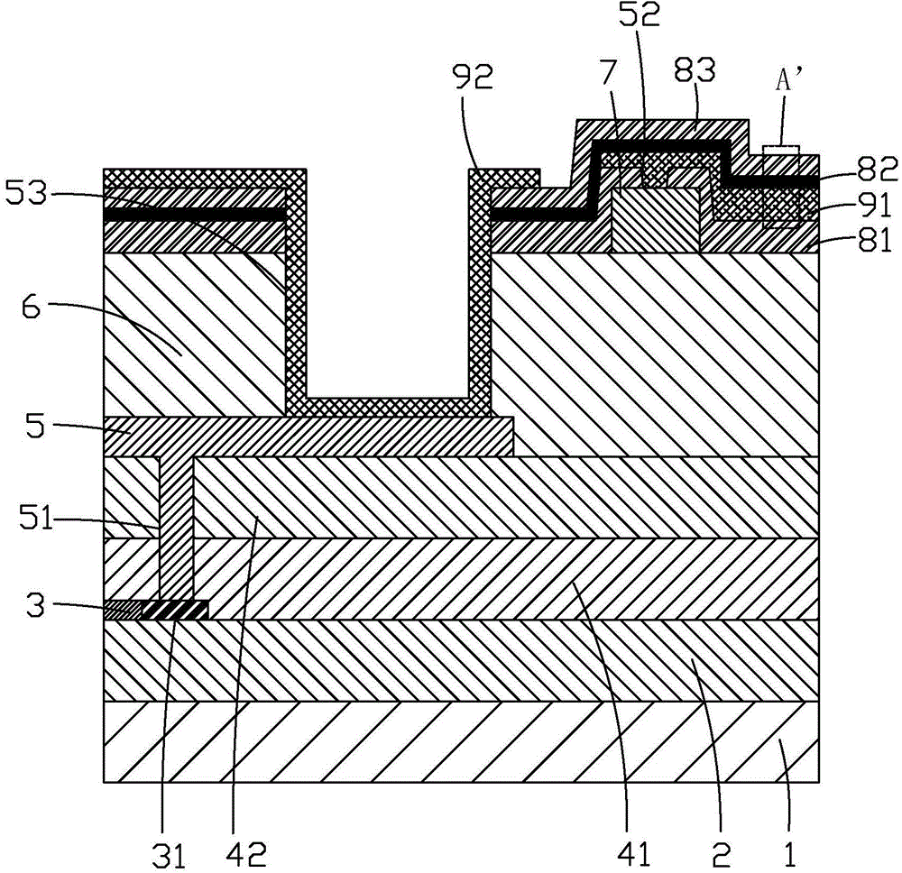
[0058] see image 3 and Figure 4 , the present invention provides an array substrate structure for a touch display panel, which includes a substrate 1, a buffer layer 2 disposed on the substrate 1, a semiconductor layer 3 disposed on the buffer layer 2, and a semiconductor layer disposed on the buffer layer 2. The gate insulating layer 41 on the buffer layer 2 and the semiconductor layer 3, the interlayer dielectric layer 42 disposed on the gate insulating layer 41, the source / drain disposed on the interlayer dielectric layer 42 5. The flat layer 6 disposed on the source / drain 5 and the interlayer dielectric layer 42, the second metal layer 7 disposed on the flat layer 6, the second metal layer 7 disposed on the flat layer The first insulat...


PUM


Abstract

The invention provides an array substrate structure and a production method thereof. According to the production method of the array substrate structure, after a common electrode (91) is formed, an anti-reduction layer (82) is formed on the common electrode (91) before a second insulating layer (83) is deposited, and therefore, a situation in which an reducing atmosphere generated in a process in which the second insulating layer (83) is directly deposited on the common electrode (91) changes the quality of the film layer of the common electrode (91) can be avoided, and influence of the deposition of the second insulating layer (83) on the common electrode (91), on the transmittance of the common electrode (91), can be decreased, and high transmittance of the common electrode (91) can be ensured, and a display effect can be improved.

Description

technical field [0001] The present invention relates to the field of display technology, in particular to an array substrate structure and a manufacturing method thereof. Background technique [0002] The touch screen monitor (Touch Screen) allows the user to operate the host computer as long as the icon or text on the computer display screen is lightly touched with a finger, thus getting rid of the keyboard and mouse operation and making the human-computer interaction more straightforward. It is mainly used for information inquiry in public halls, leadership offices, electronic games, ordering songs and dishes, multimedia teaching, air tickets, train ticket pre-sales, etc. The products are mainly divided into three categories: capacitive touch screen, resistive touch screen and surface acoustic wave touch screen. [0003] The array substrate is an important part of the touch display panel. [0004] see figure 1 , is a schematic cross-sectional view of an existing array s...

Claims


Application Information

Patent Timeline
IPC IPC(8): H01L27/12H01L21/77G06F3/041
CPCG02F1/136227H01L27/1248H01L27/1259G02F1/133345G02F1/13338H01L27/124G02F1/13685G02F1/134309G02F1/13439G02F1/136286G02F1/1368G02F2201/121G02F2202/09
Inventor 虞晓江杜海波
Owner SHENZHEN CHINA STAR OPTOELECTRONICS TECH CO LTD
Features
  • R&D
  • Intellectual Property
  • Life Sciences
  • Materials
  • Tech Scout
  • Unparalleled Data Quality
  • Higher Quality Content
  • 60% Fewer Hallucinations
Learn More