Method of forming semiconductor device

A semiconductor and device technology, applied in the field of semiconductor device formation, can solve problems such as the influence of transistor drive current, and achieve the effects of enhanced drive current, improved performance, and reduced contact resistance

Active Publication Date: 2018-02-16
SEMICON MFG INT (SHANGHAI) CORP
View PDF7 Cites 0 Cited by
  • Summary
  • Abstract
  • Description
  • Claims
  • Application Information

AI Technical Summary

Problems solved by technology

[0005] However, in the prior art, the contact resistance between the conductive plug and the source region or the drain region is relatively large, and as the size of semiconductor devices continues to shrink, the contact resistance has a particularly significant impact on the driving current of the transistor.

Method used


Image

  • Method of forming semiconductor device
  • Method of forming semiconductor device
  • Method of forming semiconductor device

Examples


Embodiment Construction

[0032] As mentioned in the background art, the contact resistance between the conductive plug and the source region or the drain region is relatively large, which easily reduces the driving current of the transistor and deteriorates the performance of the transistor.

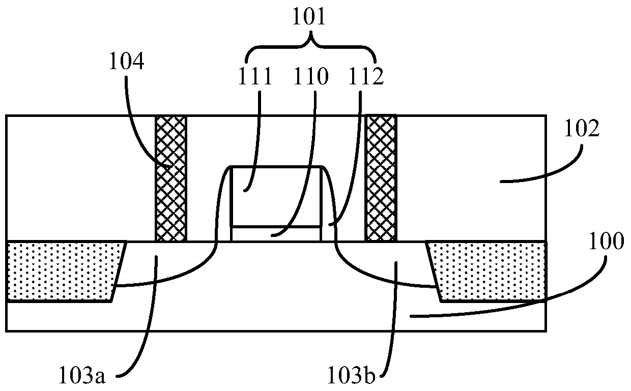
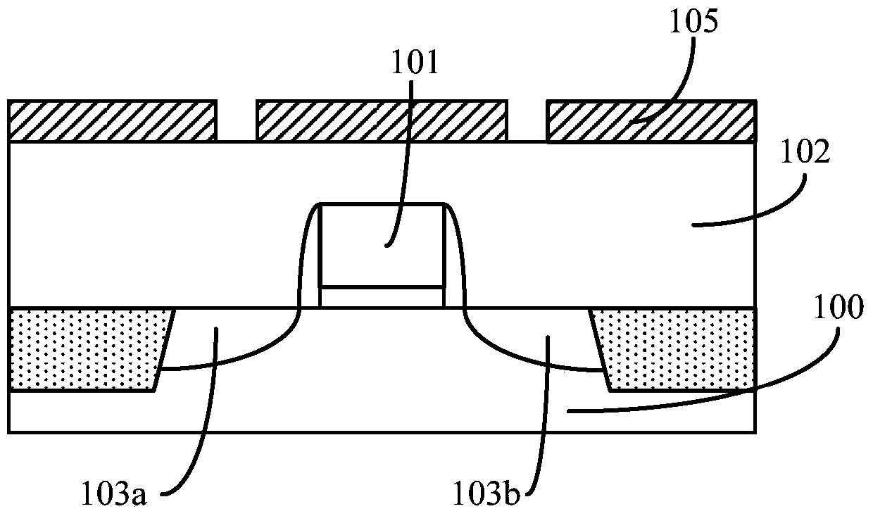
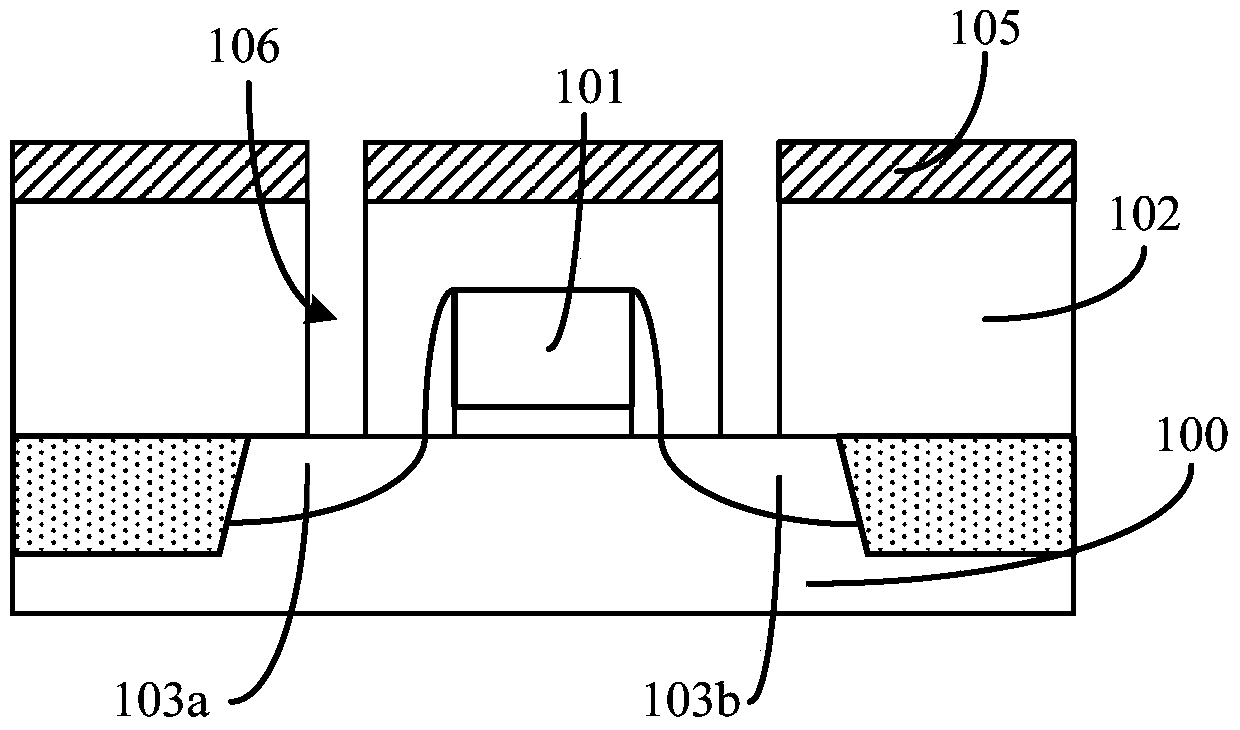
[0033] After research, it was found that during the process of forming the conductive plug, it is easy to cause damage to the surface of the source region and the drain region, resulting in the deterioration of the morphology of the contact interface between the conductive plug and the source region or the drain region, resulting in the formation of the conductive plug. The contact resistance to the source or drain region increases. For details, please refer to Figure 2 to Figure 4 , is a cross-sectional structure of a process of forming conductive plugs on the surface of the source region and the drain region.

[0034] Please refer to figure 2 , the surface of the substrate 100 has a gate structure 101, the s...


PUM


Abstract

Provided is a semiconductor device forming method which comprises: providing a substrate, wherein the surface of the substrate is equipped with a gate electrode structure, a source region and a drain region are arranged in the substrate on both sides of the gate electrode structure, the surface of the source region and the surface of the drain region are equipped with a stop layer, the surface of the substrate, the surface of the gate electrode structure, and the surface of the stop layer are equipped with a dielectric layer, and the material of the stop layer and material of the dielectric layer are different; etching a part of the dielectric layer until the surface of the stop layers is exposed so as to form a first opening in the dielectric layer; treating the stop layer on the bottom of the first opening by using an amorphization process in order that the stop layer on the bottom of the first opening forms an amorphization layer, wherein the density of the amorphization layer is less than that of the stop layer not subjected to the amorphization process; removing the amorphization layer on the bottom of the first opening and exposing the surface of the source region, the surface of the drain region, the surface of the sidewall of the stop layer, wherein the surface of the sidewall of the stop layer on the bottom of the first opening is flush with the surface of the dielectric layer of the sidewall of the first opening; and forming a conductive structure in the first opening. The performance of a semiconductor device formed by using the method is improved.

Description

technical field [0001] The invention relates to the technical field of semiconductor manufacturing, in particular to a method for forming a semiconductor device. Background technique [0002] With the rapid development of integrated circuit manufacturing technology, the size of semiconductor devices in integrated circuits, especially MOS (Metal Oxide Semiconductor, metal-oxide-semiconductor) transistors, is continuously reduced to meet the miniaturization and development of integrated circuits. Integration requirements. [0003] Please refer to figure 1 , figure 1 It is a schematic cross-sectional structure diagram of a transistor, including: a gate structure 101 located on the surface of the substrate 100, and the gate structure 101 includes: a gate dielectric layer 110 located on the surface of the substrate 100, a gate located on the surface of the gate dielectric layer 110 layer 111, and the side wall 112 located on the side wall surface of the gate dielectric layer 1...

Claims


Application Information

Patent Timeline
Patent Type & Authority Patents(China)
IPC IPC(8): H01L21/336H01L21/265
CPCH01L21/02109H01L21/265H01L29/66477
Inventor 傅丰华虞肖鹏洪中山
Owner SEMICON MFG INT (SHANGHAI) CORP
Why Eureka
Try Eureka