

Semiconductor processing device
A processing equipment and semiconductor technology, which is applied in semiconductor/solid-state device manufacturing, electrical components, circuits, etc., can solve the problems of reaction chamber 101 pollution, etc., and achieve the effect of reducing accumulation and avoiding returning to the reaction chamber
- Summary
- Abstract
- Description
- Claims
- Application Information
AI Technical Summary
Problems solved by technology
Method used
Image

Examples
Embodiment Construction
[0026] In order for those skilled in the art to better understand the technical solutions of the present invention, the semiconductor processing equipment provided by the present invention will be described in detail below in conjunction with the accompanying drawings.
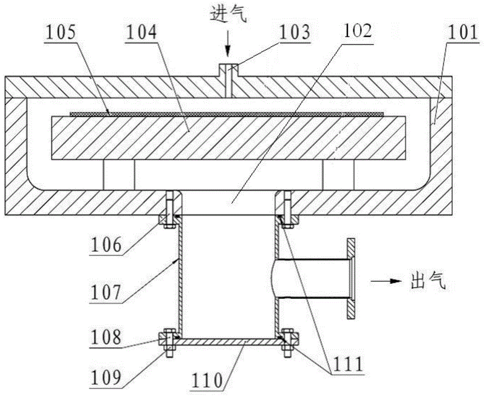
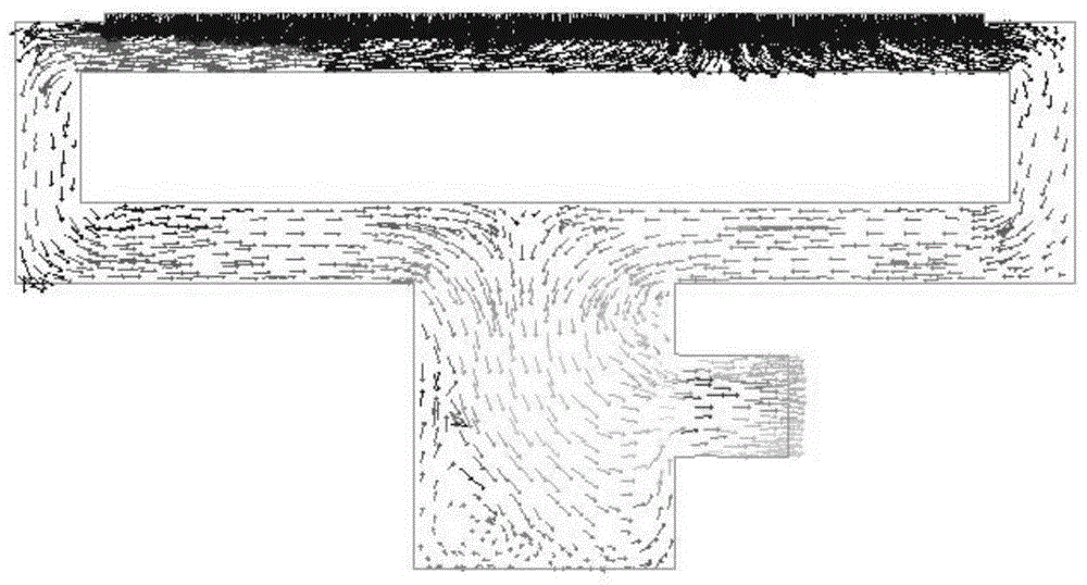
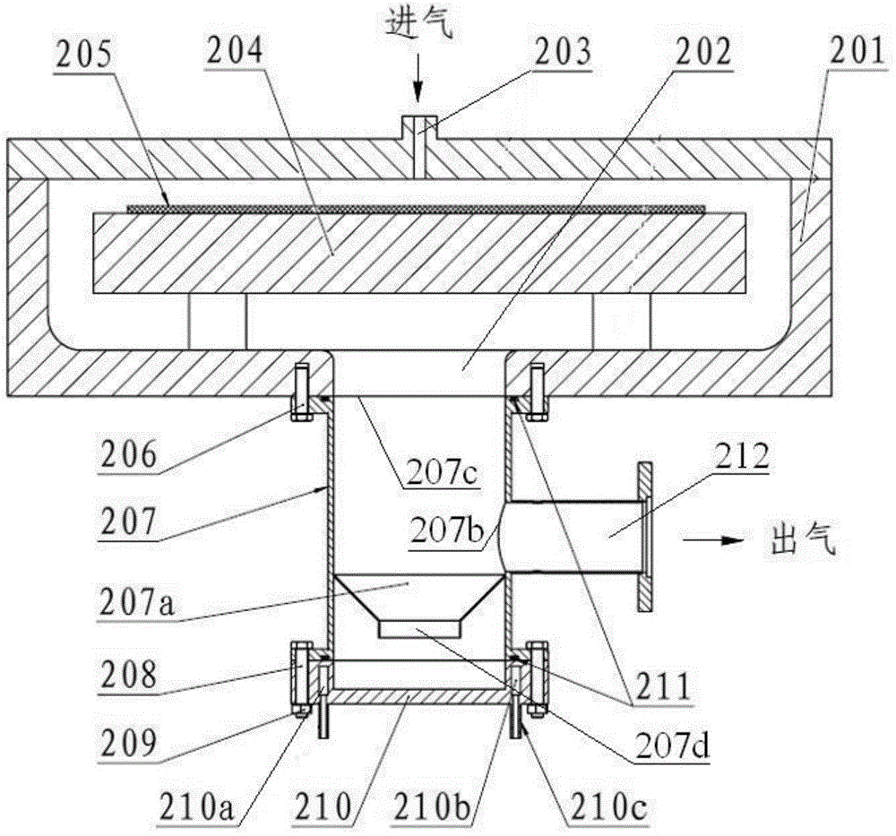
[0027] image 3 A cross-sectional view of the semiconductor processing equipment provided by the embodiment of the present invention. see image 3 , The semiconductor processing equipment provided by the embodiment of the present invention includes a reaction chamber 201 , an air extraction chamber 207 and an air extraction system disposed at the bottom of the reaction chamber 201 . Wherein, an exhaust port 202 is provided at the bottom of the reaction chamber 201, and an air inlet 207c is correspondingly provided at the top of the pumping chamber 207, and the air inlet 207c is connected with the exhaust port 202; A gas outlet 207b is provided on the side wall of the chamber 207; the gas outlet 207b is conne...
PUM
 Abstract
Description
Claims
Application Information