VDMOS device and manufacturing method thereof
A device and control gate technology, which is applied in the field of VDMOS devices and its manufacturing, can solve the problems of reduced withstand voltage, increased on-resistance, and increased process complexity, and achieve the effect of reducing Miller capacitance and on-resistance
- Summary
- Abstract
- Description
- Claims
- Application Information
AI Technical Summary
Problems solved by technology
Method used
Image

Examples
Embodiment Construction
[0038] Below in conjunction with accompanying drawing, describe technical scheme of the present invention in detail:
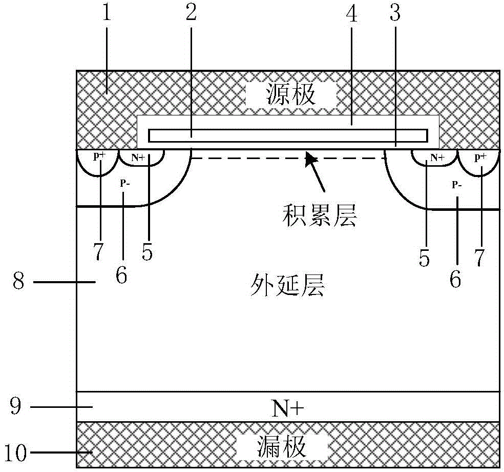
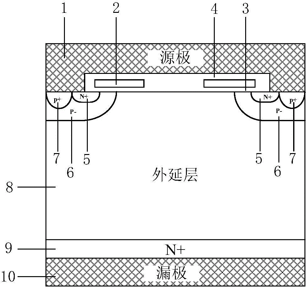
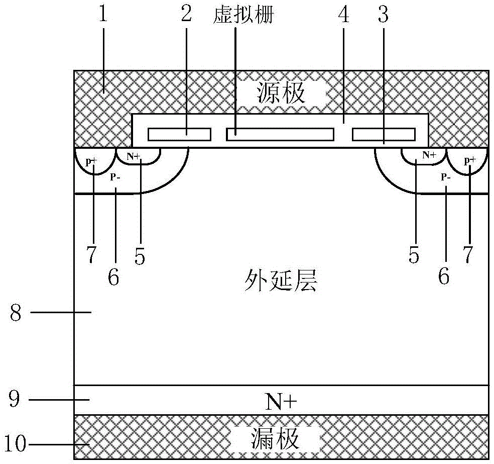
[0039] The present invention proposes a VDMOS device, such as Figure 5 As shown, it includes a semiconductor substrate 9 of the first conductivity type and a semiconductor epitaxial layer 8 of the first conductivity type arranged on the upper surface of the semiconductor substrate 9 of the first conductivity type. The bottom and the drain electrode of the semiconductor substrate 9 of the first conductivity type The metal electrode 10 is connected; the two ends of the upper layer of the first conductivity type semiconductor epitaxial layer 8 have a second conductivity type semiconductor body region 6, and the second conductivity type semiconductor body region 6 has a first conductivity type semiconductor source region 5 and a second conductivity type semiconductor body region. The second conductivity type semiconductor body contact region 7; the first conductivi...
PUM
 Abstract
Description
Claims
Application Information
 - R&D Engineer
- R&D Manager
- IP Professional
- Industry Leading Data Capabilities
- Powerful AI technology
- Patent DNA Extraction
Browse by: Latest US Patents, China's latest patents, Technical Efficacy Thesaurus, Application Domain, Technology Topic.
© 2024 PatSnap. All rights reserved.Legal|Privacy policy|Modern Slavery Act Transparency Statement|Sitemap