

Method for fabricating trench power device
a power device and trench technology, applied in the direction of semiconductor devices, electrical equipment, basic electric elements, etc., can solve the problems of lower efficiency and higher gate charge, and achieve the effect of reducing miller capacitance and reducing rc delay
- Summary
- Abstract
- Description
- Claims
- Application Information
AI Technical Summary
Benefits of technology
Problems solved by technology
Method used
Image

Examples
Embodiment Construction
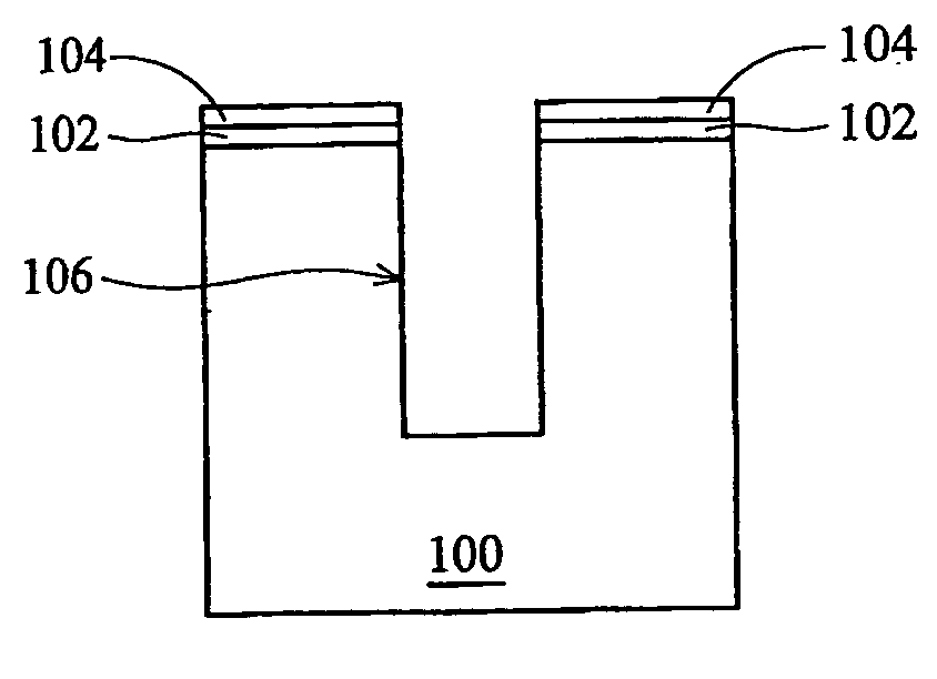
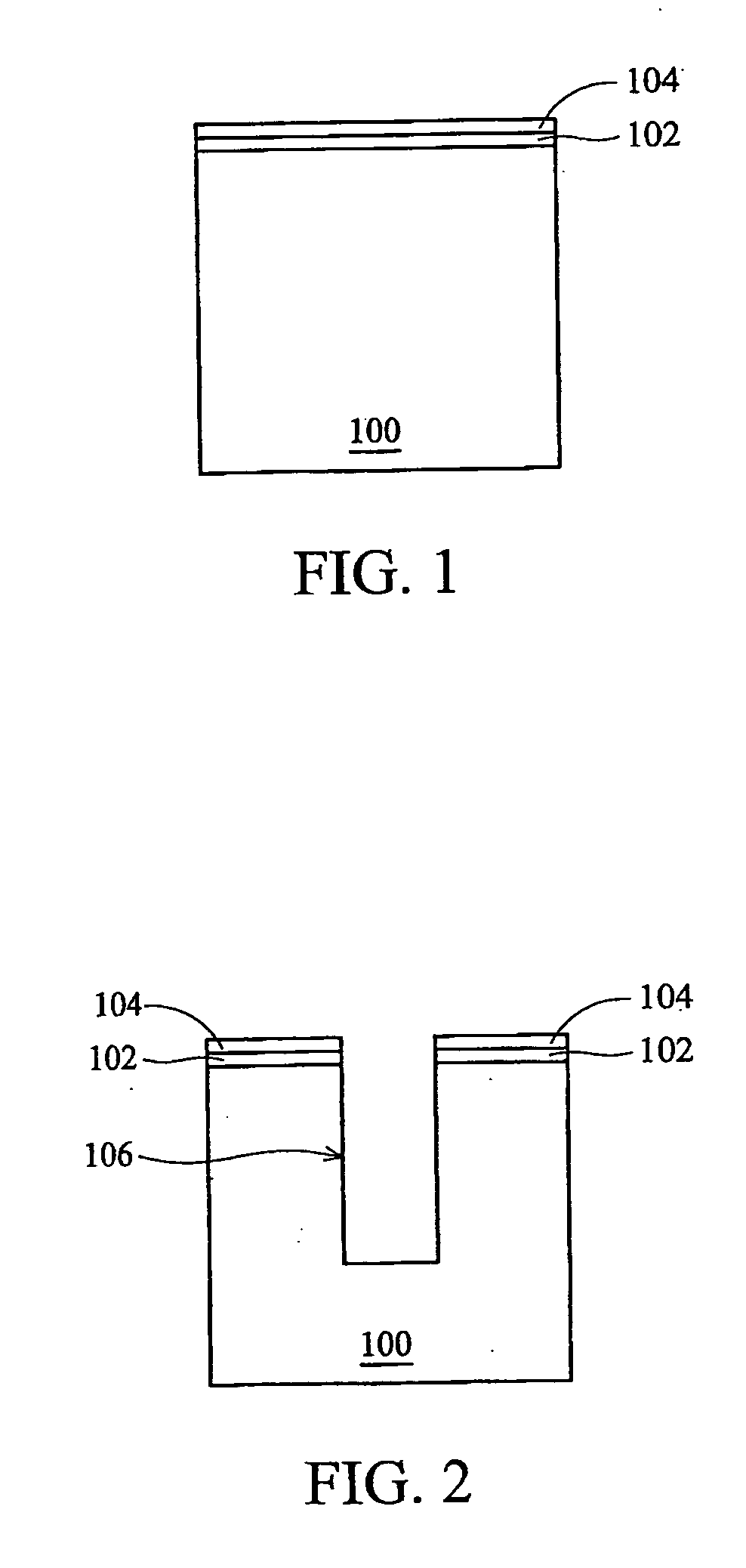
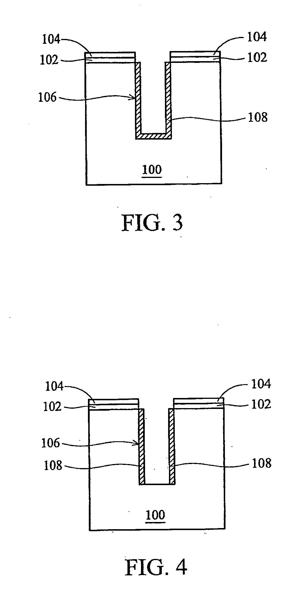
[0013] Referring to FIG. 1, a substrate 100 is provided. The substrate 100 can be a bare silicon substrate, a P-type doped silicon substrate, or an N-type doped substrate. Alternatively, the substrate 100 can also have printed alignment marks for lithography. An oxide layer 102 is formed on the substrate 100. The oxide layer 102 can be formed by thermal oxidation, for example. A silicon nitride layer 104 is consecutively formed on the oxide layer 102. The silicon nitride layer 104 can be formed by chemical vapor deposition (CVD), for example.
[0014] The stress of the silicon nitride layer 104 is relieved by the oxide layer 102. The oxide layer 102 can also be omitted if the stress is not an important issue.
[0015] According to an embodiment of the invention, the silicon nitride layer 104 is formed by a chemical vapor deposition at a temperature in a range of approximately 700 to 800° C., at a pressure in a range of approximately 0.2 to 0.5 torr, with SiH2Cl2 at a flow rate in a rang...
PUM
 Abstract
Description
Claims
Application Information