Ring ion injection method, semiconductor device and manufacture method thereof

An ion implantation, ring-shaped technology, applied in semiconductor/solid-state device manufacturing, semiconductor devices, electrical components, etc., can solve the problem of reducing the frequency response characteristics of common-source operational amplifiers, and achieve improved frequency response characteristics, other performance maintenance, The effect of reducing parasitic overlap capacitance

Inactive Publication Date: 2012-08-01
SHANGHAI HUALI MICROELECTRONICS CORP
View PDF4 Cites 3 Cited by
  • Summary
  • Abstract
  • Description
  • Claims
  • Application Information

AI Technical Summary

Problems solved by technology

At the same time, the ring-shaped ion implantation also determines the size of the overlapping area between the drain dopant ions and the gate. The larger the overlapping area, the greater the parasitic overlapping capacitance, which will cause more serious Miller effect. , which leads to the reduction of the frequency response characteristics of the common-source operational amplifier, therefore, how to improve the frequency response effect of the common-source operational amplifier by controlling the annular ion implantation method has become the focus of research in this field

Method used


Image

  • Ring ion injection method, semiconductor device and manufacture method thereof
  • Ring ion injection method, semiconductor device and manufacture method thereof
  • Ring ion injection method, semiconductor device and manufacture method thereof

Examples


Embodiment Construction

[0015] In order to make the above objects, features and advantages of the present invention more comprehensible, specific implementations of the present invention will be described in detail below in conjunction with the accompanying drawings.

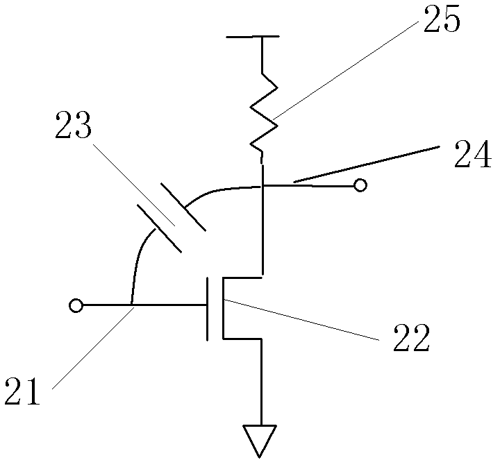
[0016] The present invention provides a ring-shaped ion implantation method, please refer to Figures 4A-4E , taking the NMOS (N-type Metal Oxide Semiconductor) transistor in the CMOS device technology as an example, the ring-shaped ion implantation method includes the following steps:

[0017] Please refer to Figure 4A , first provide a substrate 401, on which a gate structure 402 is formed, the substrate 401 includes a source region and a drain region, and the source region refers to the source extension region, source The metallurgical junction of the electrode and the region of the heavily doped source region. Similarly, the drain region refers to the region where the drain extension region, the metallurgical junction of the drai...


PUM


Abstract

The invention provides a ring ion injection method which comprises the steps of: respectively carrying out ion injection on a source electrode and a drain electrode on a substrate, wherein an included angle of a drain electrode ion injection direction and a direction vertical to the surface of the substrate is more than that of a source electrode ion injection direction and the direction vertical to the surface of the substrate; and enabling a charge region of a drain electrode space to be compressed from a trench direction so that an overlapping area of the drain electrode and a grid electrode is compressed, thus a parasitic overlap capacitance between the drain electrode and the grid electrode of a semiconductor device is decreased, a Miller capacitance of a common-source amplifier is reduced, and the frequency response characteristic of the common-source amplifier is improved. In addition, though the charge region of the drain electrode space is compressed, a charge region of a source electrode space extends into a trench, the effective trench length of the semiconductor device is basically kept unchangeable, and other properties of the semiconductor device can be maintained.

Description

technical field [0001] The invention relates to the field of semiconductor manufacturing, in particular to a ring-shaped ion implantation method, a semiconductor device and a manufacturing method thereof. Background technique [0002] CMOS (Complementary Metal Oxide Semiconductor) operational amplifier is one of the basic units of various circuits. With the development of information technology, the requirements for the processing speed of information data are getting higher and higher, and the requirements for the frequency response characteristics of the CMOS operational amplifiers used in it are also getting higher and higher. However, the parasitic capacitance of CMOS devices plays an increasingly negative role with the increase of operating frequency. How to reduce the influence of these parasitic capacitances on CMOS operational amplifiers has become the key to improving the frequency response characteristics of CMOS operational amplifiers. [0003] Miller capacitance...

Claims


Application Information

Patent Timeline
Patent Type & Authority Applications(China)
IPC IPC(8): H01L21/265H01L21/336H01L29/78
Inventor 俞柳江
Owner SHANGHAI HUALI MICROELECTRONICS CORP
Why Eureka
Try Eureka