Bidirectional IGBT and manufacturing method therefor

An N-type, positive technology, applied in the manufacture of semiconductor/solid-state devices, electrical components, circuits, etc., can solve the problems affecting the compromise characteristics of device switching loss, the deterioration of the short-circuit safe working area of ​​the device, and the increase of the saturation current density of the device. Achieve the effect of increasing the breakdown voltage, improving the short-circuit safe working area, and increasing the switching speed

Inactive Publication Date: 2018-03-06
UNIV OF ELECTRONICS SCI & TECH OF CHINA
View PDF5 Cites 4 Cited by
  • Summary
  • Abstract
  • Description
  • Claims
  • Application Information

AI Technical Summary

Problems solved by technology

[0007] The implementation of method (1) will increase the gate-emitter capacitance and gate-collector capacitance at the same time, and the switching process of the IGBT is essentially the process of charging / discharging the gate capacitance, so the increase in the gate capacitance will Makes the charging / discharging time longer, which in turn causes the switching speed to decrease
Therefore, the deep trench gate depth will reduce the switching speed of the device, increase the switching loss of the device, and affect the compromise characteristics of the device's conduction voltage drop and switching loss; and the implementation of method (2) will increase the device's switching loss The gate capacitance will reduce the switching speed of the device and increase the switching loss, which will affect the compromise between the conduction voltage drop and switching loss of the device. On the other hand, the large channel density will also increase the saturation current density of the device, making the device short-circuit safe. work area deterioration
Additionally, for figure 1 In the bidirectional IGBT structure shown, the gate oxide layer is formed in the trench by one thermal oxidation. In order to ensure a certain threshold voltage, the thickness of the entire gate oxide layer is small. Since the MOS capacitance is inversely proportional to the thickness of the oxide layer, traditional The small gate oxide thickness in the bidirectional IGBT structure greatly increases the gate capacitance of the device
In addition, the small gate oxide thickness concentrates the electric field at the bottom of the trench, making the device less reliable

Method used


Image

  • Bidirectional IGBT and manufacturing method therefor
  • Bidirectional IGBT and manufacturing method therefor
  • Bidirectional IGBT and manufacturing method therefor

Examples


Embodiment 1

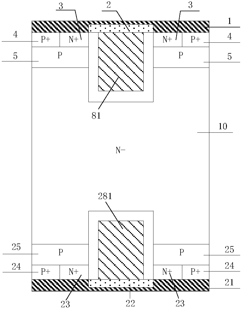
[0067] This embodiment provides a bidirectional IGBT whose cell structure is as follows image 3As shown, it includes an N-channel MOS structure symmetrically arranged on both sides of the N-type drift region 10; the front-side MOS structure includes: a front-side emitter metal 1, a first front-side dielectric layer 22, a second front-side dielectric layer 20, and a front-side split trench Groove gate structure, front P+ emitter region 3, front N+ emitter region 4, front P-type base region 5, front N-type charge storage layer 6 and front P-type body region 9; the back MOS structure includes: back emitter metal 21, the first A rear dielectric layer 222, a second rear dielectric layer 220, a rear split trench gate structure, a rear P+ emission region 23, a rear N+ emission region 24, a rear P-type base region 25, a rear N-type charge storage layer 26 and a rear P-type body region 29; characterized in that:

[0068] The front split trench gate structure is located in the middle ...

Embodiment 2

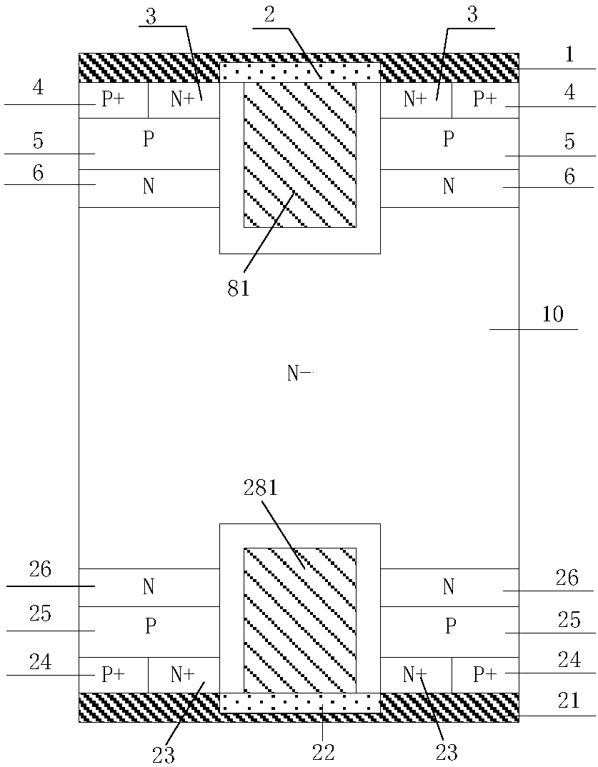
[0071] This embodiment provides a bidirectional IGBT whose cell structure is as follows Figure 4 As shown, the difference of this embodiment compared with Embodiment 1 is that the thickness of the sidewall of the split electrode dielectric layer below the N-type charge storage layer 6 and close to the side of the N-type charge storage layer is greater than that under the N-type charge storage layer 6 and away from it. The thickness of the sidewall of the split electrode dielectric layer on the side of the N-type charge storage layer, the rear split trench gate structure and the front split trench gate structure are arranged symmetrically up and down along the lateral centerline of the N-type drift region 10 .

[0072] This embodiment increases the thickness of the dielectric layer at the bottom of the trench, further improves the electric field concentration at the bottom of the trench, and increases the breakdown voltage of the device.

Embodiment 3

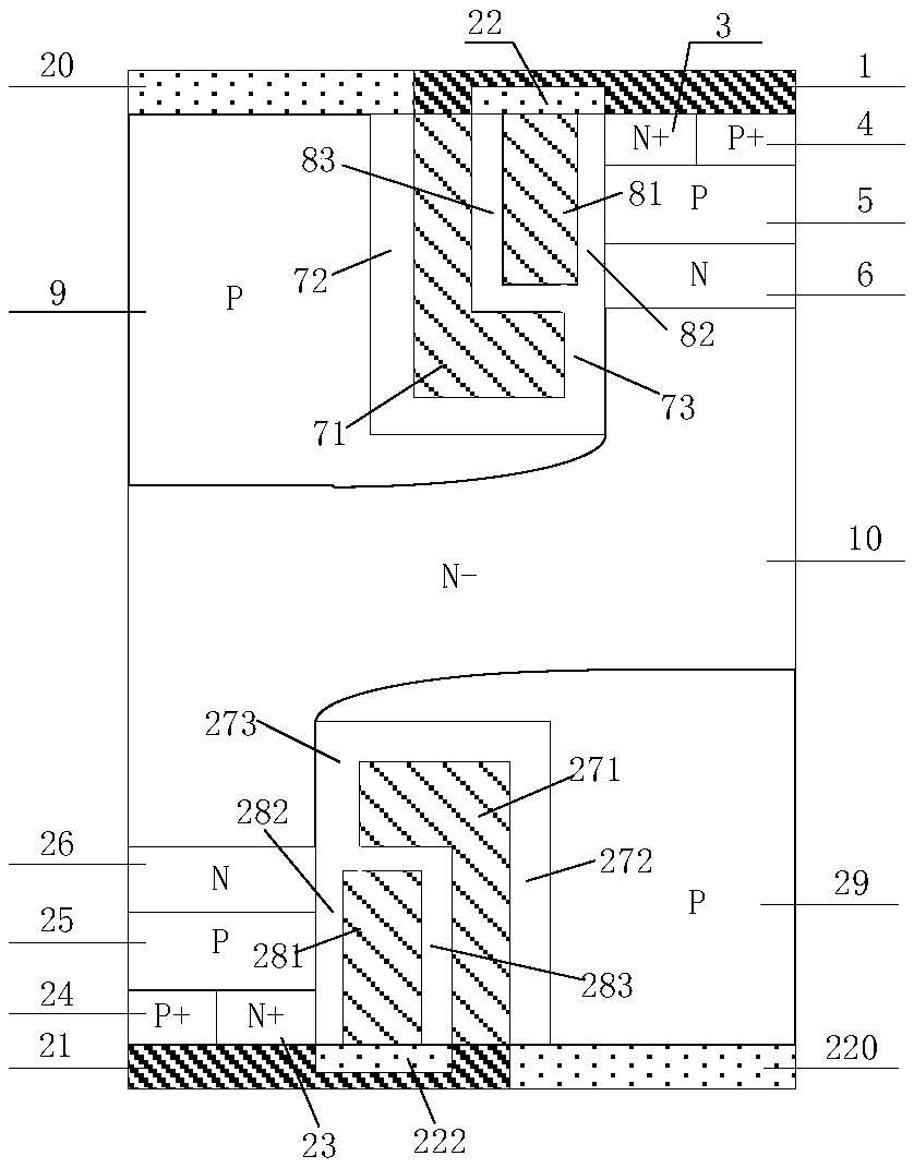
[0074] This embodiment provides a bidirectional IGBT whose cell structure is as follows Figure 5 As shown, the difference of this embodiment compared with the first embodiment is that: the front MOS structure and the back MOS structure are completely mirror-symmetrically arranged up and down along the lateral centerline of the N-type drift region 10 .


PUM


Abstract

The invention discloses a bidirectional IGBT and a manufacturing method therefor, and belongs to the technical field of power semiconductor devices. According to the invention, a split electrode whichis equipotential with a surface metal and a thick dielectric layer located at a peripheral side of the split electrode are introduced to a conventional trench gate structure, and a floating P-type body region is introduced to one side of a split trench gate structure, thereby achieving the symmetric forwarding and reverse on/off characteristics of an IGBT structure under the condition that a threshold voltage and connection of an IGBT device are not affected. The adverse effect caused by the Miller effect is improved, and the drive power consumption is reduced. The current and voltage oscillation and EMI problems are avoided in a start dynamic process of the device. The short-circuit safety working area of the device is improved. The gate capacitance is reduced, the switching speed of thedevice is improved, and the switching loss of the device is reduced. The concentration of an electric field at the bottom of a trench is improved, and the breakdown voltage of the device is improved.The carrier enhancement effect of an emitter electrode is improved, the carrier concentration distribution of the whole N-type drift region is improved, and the compromise between the forwarding conduction voltage drop and switching-off loss is improved.

Description

technical field [0001] The invention belongs to the technical field of power semiconductor devices, and relates to an insulated gate bipolar transistor (IGBT), in particular to a bidirectional IGBT and a manufacturing method thereof. Background technique [0002] A new type of power electronic device composed of an insulated gate bipolar transistor (IGBT), an insulated field effect transistor (MOSFET) and a bipolar junction transistor (BJT), can be equivalent to a MOSFET driven by a bipolar junction transistor. IGBT combines the working mechanism of MOSFET structure and bipolar junction transistor. It not only has the advantages of MOSFET easy to drive, low input impedance, and fast switching speed, but also has the advantages of BJT on-state current density, low on-state voltage, low loss, and stability. Therefore, compared with current-controlled devices such as thyristors, it has obvious advantages in controllability, safe operating area, switching loss and simplification...

Claims


Application Information

Patent Timeline
Patent Type & Authority Applications(China)
IPC IPC(8): H01L29/739H01L29/423H01L29/08H01L29/06H01L21/331
CPCH01L29/0657H01L29/0804H01L29/4236H01L29/42364H01L29/66348H01L29/7397
Inventor 张金平赵倩蔡羽恒刘竞秀李泽宏任敏张波
Owner UNIV OF ELECTRONICS SCI & TECH OF CHINA
Why Eureka
Try Eureka