Semiconductor device with reduced miller capacitance and fabrication method thereof

A device and power semiconductor technology, applied in the field of metal-oxide-semiconductor field-effect transistor devices and their fabrication, can solve problems such as slow switching speed

Inactive Publication Date: 2014-06-04
ANPEC ELECTRONICS CORPORATION
View PDF3 Cites 4 Cited by
  • Summary
  • Abstract
  • Description
  • Claims
  • Application Information

AI Technical Summary

Problems solved by technology

[0003] In order to reduce the resistance of the above-mentioned area, the trench type power device (UMOS) was proposed, and because the UMOS structure does not exist in the JFET area, the unit size of the UMOS device can be reduced to increase the channel density (channel density), which can further reduce On-resistance, but on the other hand, UMOS devices also increase the gate-drain capacitance (Miller capacitance) due to their structure, which slows down the switching speed

Method used


Image

  • Semiconductor device with reduced miller capacitance and fabrication method thereof
  • Semiconductor device with reduced miller capacitance and fabrication method thereof
  • Semiconductor device with reduced miller capacitance and fabrication method thereof

Examples


Embodiment Construction

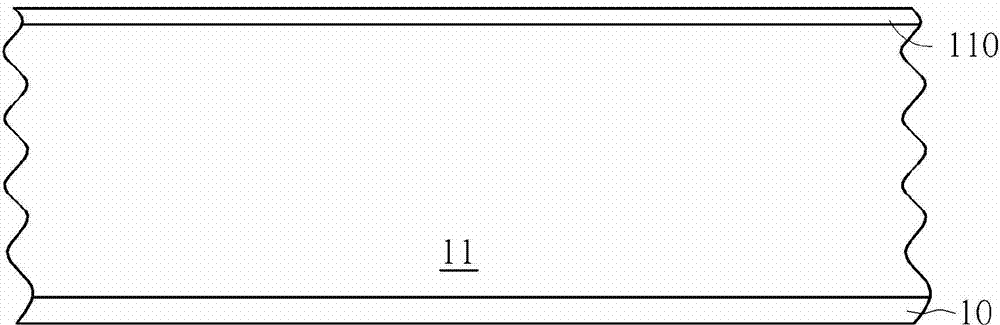
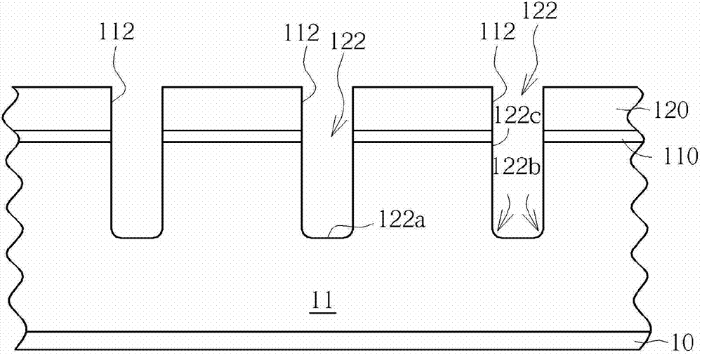
[0022] see Figure 1 to Figure 8 , which is a schematic diagram of a method for manufacturing a trench-type power transistor device according to an embodiment of the present invention. First, if figure 1 As shown, a semiconductor substrate 10 is provided, such as an N-type heavily doped silicon substrate, which can be used as a drain of a transistor device. Next, an epitaxial layer 11 , such as an N-type epitaxial silicon layer, is formed on the semiconductor substrate 10 by an epitaxial process. Next, a cushion layer 110 , for example, a silicon oxide cushion layer, may be formed on the surface of the epitaxial layer 11 .

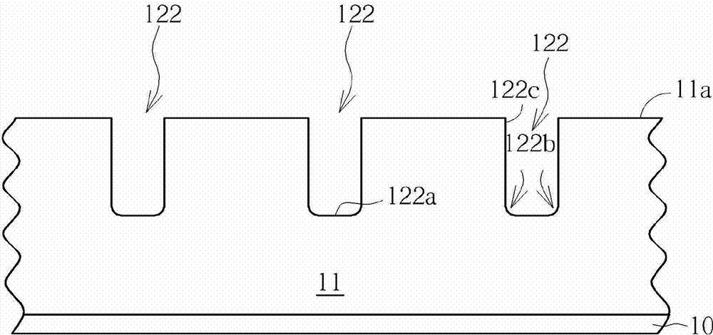
[0023] Such as figure 2 As shown, a hard mask layer 120 such as a silicon nitride layer is deposited on the epitaxial layer 11, and then an opening 112 is formed in the hard mask layer 120 by using photoresist and photolithography. Then the photoresist is removed, and then, the epitaxial layer 11 is etched to a predetermined depth through the opening ...


PUM


Abstract

A semiconductor power device includes an epitaxial layer grown on a semiconductor substrate; an ion well with a junction depth in the epitaxial layer; a gate trench with a depth deeper than the junction depth in the ion well; a gate oxide layer in the gate trench; a gate embedded the gate trench; and a pocket doping region in the epitaxial layer. The pocket doping region is adjacent to and covers at least a corner of the gate trench.

Description

technical field [0001] The present invention generally relates to the technical field of semiconductor devices, in particular to a metal oxide field effect transistor (MOSFET) device with low Miller capacitance and a manufacturing method thereof. Background technique [0002] In traditional power transistors, planar power devices (DMOS) make the on-resistance (on -resistance) rises. [0003] In order to reduce the resistance of the above-mentioned area, the trench type power device (UMOS) was proposed, and because the UMOS structure does not exist in the JFET area, the unit size of the UMOS device can be reduced to increase the channel density (channel density), which can further reduce On-resistance, but on the other hand, UMOS devices also increase the gate-drain capacitance (Miller capacitance) due to their structure, which slows down the switching speed. Contents of the invention [0004] Therefore, the object of the present invention is to provide a power semiconduc...

Claims


Application Information

Patent Timeline
Patent Type & Authority Applications(China)
IPC IPC(8): H01L29/78H01L29/10H01L21/336
CPCH01L29/7827H01L29/1037H01L29/4236H01L29/66666H01L29/41766H01L29/66734H01L29/7813H01L29/1095H01L29/66727H01L29/0878
Inventor 林永发
Owner ANPEC ELECTRONICS CORPORATION
Why Eureka
Try Eureka