Method and system of calculating piezoelectric charge distribution at piezoelectric electronics device interface

A technology of electro-electronics and piezoelectric charge, applied in the field of calculating the distribution of piezoelectric charges at the interface of piezoelectric electronic devices, to achieve the effect of optimizing functions and accelerating the process of industrialization

Active Publication Date: 2015-11-25
BEIJING INST OF NANOENERGY & NANOSYST
View PDF7 Cites 0 Cited by
  • Summary
  • Abstract
  • Description
  • Claims
  • Application Information

AI Technical Summary

Problems solved by technology

[0003] The purpose of the present invention is to provide a method and system for calculating the piezoelectric charge distribution at the interface of piezoelectric electronic devices, which is used to solve the problem of calculating the piezoelectric charge distribution of piezoelectric electronic devices, especially the piezoelectric charge distribution at the interface

Method used


Image

  • Method and system of calculating piezoelectric charge distribution at piezoelectric electronics device interface
  • Method and system of calculating piezoelectric charge distribution at piezoelectric electronics device interface
  • Method and system of calculating piezoelectric charge distribution at piezoelectric electronics device interface

Examples


Embodiment Construction

[0028] Specific embodiments of the present invention will be described in detail below in conjunction with the accompanying drawings. It should be understood that the specific embodiments described here are only used to illustrate and explain the present invention, and are not intended to limit the present invention.

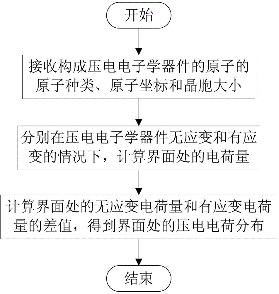
[0029] figure 1 It is a flow chart of the method for calculating piezoelectric charge distribution at the interface of piezoelectric electronic devices provided by the present invention, such as figure 1 As shown, the method includes: receiving the atomic species, atomic coordinates and unit cell size of the atoms constituting the piezoelectric electronic device; species, atomic coordinates, and unit cell size to calculate the amount of charge at the interface, where in the case of no strain, the amount of charge is the amount of unstrained charge, and in the case of strain, the amount of charge is the amount of strained charge amount; and calculating the diff...


PUM


Abstract

The present invention discloses a method and system of calculating the piezoelectric charge distribution at a piezoelectric electronics device interface. The method comprises the steps of receiving the atomic species, the atomic coordinate and the cell dimension of the atoms forming a piezoelectric electronics device; calculating the quantity of electric charge at the interface separately on the conditions that the piezoelectric electronics device does not have the strain and has the strain, wherein on the condition of not having the strain, the quantity of electric charge is the strain-free quantity of electric charge, and on the condition of having the strain, the quantity of electric charge is the strain quantity of electric charge; calculating the difference of the strain-free quantity of electric charge and the strain quantity of electric charge at the interface to obtain the piezoelectric charge distribution at the interface. According to the present invention, by calculating the quantity of electric charge at the interface on the conditions that the piezoelectric electronics device does not have the strain and has the strain separately, the piezoelectric charge distribution at the interface is obtained, so that the distribution condition of the piezoelectric charges at the interface can be known accurately, and accordingly, the transport property of the piezoelectric electronics device can be simulated accurately, and helps can be provided for optimizing the functions of the piezoelectric electronics device and speeding up the piezoelectric electronics device industrialization process.

Description

technical field [0001] The present invention relates to techniques for calculating piezoelectric charge distribution of piezoelectric electronic devices, in particular, to methods and systems for calculating piezoelectric charge distribution at interfaces of piezoelectric electronic devices. Background technique [0002] The core part of piezoelectric electronic devices is piezoelectric semiconductors, such as zinc oxide, gallium nitride, indium nitride, etc. Under the action of external stress, piezoelectric charges and corresponding piezoelectric electric fields will be generated on the surface of piezoelectric semiconductors, thereby affecting the transport properties of semiconductors. Therefore, external stress can be used to replace the traditional gate electrode to regulate the transport properties of piezoelectric electronic devices, which is called piezoelectric electronics. The piezoelectric charge generated at the interface between the piezoelectric semiconductor...

Claims


Application Information

Patent Timeline
Patent Type & Authority Applications(China)
IPC IPC(8): G01R29/24
Inventor 刘伟张爱华张岩王中林
Owner BEIJING INST OF NANOENERGY & NANOSYST
Why Eureka
Try Eureka