Built-in self-capacitance touch display panel and manufacturing method thereof

一种自电容触控、显示面板的技术,应用在电数字数据处理、光学、仪器等方向,能够解决面板制程工艺难度、面板驱动成本高等问题,达到降低驱动成本的效果

Active Publication Date: 2015-11-25
TCL CHINA STAR OPTOELECTRONICS TECH CO LTD
View PDF4 Cites 26 Cited by
  • Summary
  • Abstract
  • Description
  • Claims
  • Application Information

AI Technical Summary

Problems solved by technology

[0006] Existing embedded self-capacitance touch display panels usually require a set of touch circuits (including touch scanning lines, touch receiving lines, and touch self-capacitance) and a driving control part to realize the touch function. The process is difficult, and the driving cost of the panel is relatively high

Method used


Image

  • Built-in self-capacitance touch display panel and manufacturing method thereof
  • Built-in self-capacitance touch display panel and manufacturing method thereof
  • Built-in self-capacitance touch display panel and manufacturing method thereof

Examples


Embodiment Construction

[0054] In order to further illustrate the technical means adopted by the present invention and its effects, the following describes in detail in conjunction with preferred embodiments of the present invention and accompanying drawings.

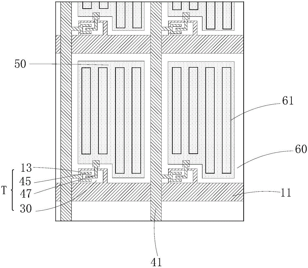
[0055] The present invention firstly provides an embedded self-capacitance touch display panel, including: an array substrate, a CF substrate, and a liquid crystal layer arranged between the array substrate and the CF substrate. side shot.

[0056] see figure 1 , the array substrate includes:

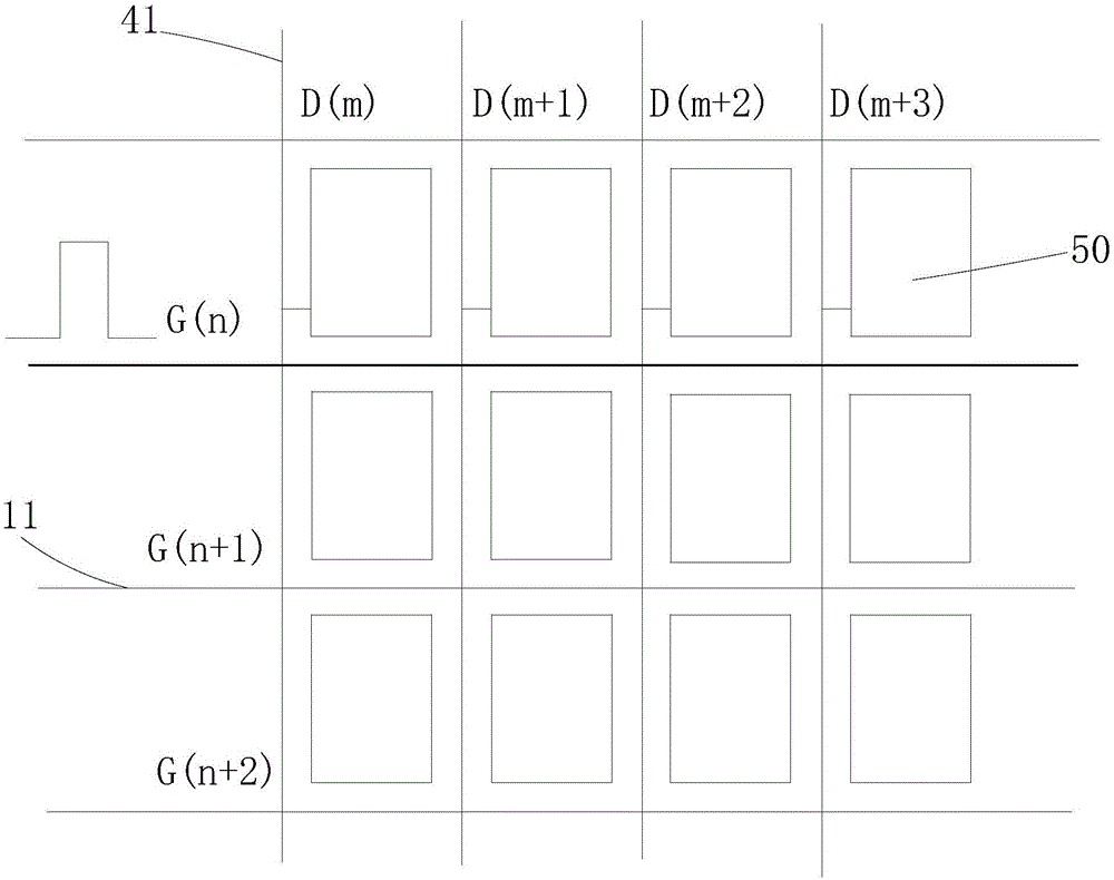
[0057] A plurality of grid scanning lines 11 arranged at intervals along the horizontal direction;

[0058] A plurality of data lines 41 arranged at intervals in the vertical direction, the plurality of gate scanning lines 11 arranged at intervals in the horizontal direction and a plurality of data lines 41 arranged at intervals in the vertical direction are insulated and interlaced with each other, dividing a plurality of sub-pixels area;

[0059] ...


PUM


Abstract

The invention provides a built-in self-capacitance touch display panel and a manufacturing method thereof. The built-in self-capacitance touch display panel comprises an array substrate, a CF substrate and a liquid crystal layer arranged between the array substrate and the CF substrate, and light enters through one side of the CF substrate and comes out through one side of the array substrate. The array substrate comprises a plurality of grid electrode scanning lines (11) arranged in the horizontal direction at intervals, a plurality of data lines (41) arranged in the vertical directions at intervals, and a plurality of pixel electrodes (50) arranged into a matrix, wherein the grid electrode scanning lines (11) also serve as touch control scanning lines, the data lines (41) also serve as touch control receiving lines, and the pixel electrodes (50) also serve as touch control self-capacitors; in this way, on the premise that the number of existing array substrate technological processes is not increased, built-in self-capacitance touch control can be achieved, and panel driving cost can be reduced. By the adoption of the manufacturing method of the built-in self-capacitance touch display panel, the number of existing array substrate technological processes is not increased, and panel driving cost is reduced.

Description

technical field [0001] The invention relates to the field of display technology, in particular to an embedded self-capacitance touch display panel and a manufacturing method thereof. Background technique [0002] With the rapid development of display technology, touch display panels have been widely accepted and used by people, for example, smart phones, tablet computers, etc. all use touch display panels. The touch display panel integrates the touch panel and the liquid crystal display panel, so that the liquid crystal display panel has the functions of displaying and sensing touch input at the same time. [0003] A liquid crystal display panel is usually composed of a color filter substrate (ColorFilter, CF), a thin film transistor array substrate (ThinFilmTransistorArraySubstrate, TFTArraySubstrate), and a liquid crystal layer (LiquidCrystalLayer) arranged between the two substrates. A driving voltage is applied to the glass substrate to control the rotation of the liqui...

Claims


Application Information

Patent Timeline
Patent Type & Authority Applications(China)
IPC IPC(8): G06F3/044G02F1/1333
CPCG02F1/13338G02F1/136286G02F2202/103G06F3/0412G06F2203/04103G06F2203/04111G06F3/04184G06F3/0443G02F1/136295G02F1/133345G02F1/133514G02F1/13439G02F1/1368G02F2201/121G02F2201/123G02F2201/50G06F3/044G06F3/04166
Inventor 徐向阳
Owner TCL CHINA STAR OPTOELECTRONICS TECH CO LTD
Why Eureka
Try Eureka