Film transistor, pixel structure, display substrate, display panel and display device

A technology of thin film transistors and pixel structures, which is applied in the fields of display substrates, display panels and display devices, pixel structures, and thin film transistors. Changes in characteristics, avoiding flickering bad effects

Active Publication Date: 2015-12-02
BOE TECH GRP CO LTD +1
View PDF4 Cites 5 Cited by
  • Summary
  • Abstract
  • Description
  • Claims
  • Application Information

AI Technical Summary

Problems solved by technology

However, for this thin film transistor, due to the asymmetry of the pattern of the source 3 and the drain 4, when the positive and negative frames are switched, the characteristics of the thin film transistor will be greatly different.
like image 3 As shown, the solid line represents the holding voltage of the pixel in the ideal state, and the dotted line represents the holding voltage of the pixel when the positive and negative frames are actually switched. It can be seen that due to the difference in the characteristics of the thin film transistor, the holding voltage of the pixel is different when the positive and negative frames are switched. Larger, which can cause flickering problems

Method used


Image

  • Film transistor, pixel structure, display substrate, display panel and display device
  • Film transistor, pixel structure, display substrate, display panel and display device
  • Film transistor, pixel structure, display substrate, display panel and display device

Examples


Embodiment Construction

[0030] Specific embodiments of the present invention will be described in detail below in conjunction with the accompanying drawings. It should be understood that the specific embodiments described here are only used to illustrate and explain the present invention, and are not intended to limit the present invention.

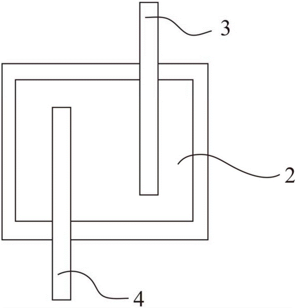
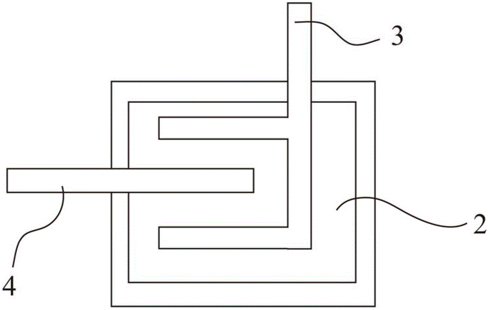
[0031] The present invention provides multiple embodiments of a thin film transistor. Figure 4 is a schematic diagram of the thin film transistor in the first embodiment. Such as Figure 4 As shown, the thin film transistor includes a gate 1, an active layer 2, a source 3 and a drain 4, the patterns of the source 3 and the drain 4 are symmetrical to each other, and the source 3 and the drain 4 The graphs are not parallel.

[0032] The patterns of the source electrode 3 and the drain electrode 4 are not parallel, which excludes the situation that the source electrode 3 and the drain electrode 4 are straight lines, that is, they are different from those in the...


PUM


Abstract

The invention provides a film transistor, a pixel structure, a display substrate, a display panel and a display device. The film transistor comprises a source electrode and a drain electrode. The center point of the source electrode and the center point of the drain electrode are symmetrical to each other in shape, and the source electrode and the drain electrode are not parallel in shape. The source electrode and the drain electrode of the film transistor are not parallel in shape, that is to say, the source electrode and the drain electrode are curves or multi-segment lines but not straight lines. Such source and drain electrodes enables the ratio of width to length (W / L) of the film transistor to be increased. In this way, the charging time for a pixel structure, charged by a data line, included in the film transistor is reduced, and the display demand is met. Meanwhile, the center point of the source electrode and the center point of the drain electrode are symmetrical to each other, so the characteristics of the film transistor are prevented from changing during switching between positive and negative frames, the sustaining voltage of pixels keeps unchanged, and unsteady flickering is avoided.

Description

technical field [0001] The present invention relates to the field of display technology, in particular to a thin film transistor, a pixel structure, a display substrate, a display panel and a display device. Background technique [0002] A thin film transistor generally includes a gate, an active layer, a source and a drain. In the field of display technology, the gate is generally connected to the gate line, the source is generally connected to the data line, and the drain is generally connected to the pixel electrode. [0003] figure 1 It is a schematic top view of a conventional thin film transistor. Such as figure 1 As shown, the source 3 and the drain 4 of the thin film transistor are linear, parallel to each other, and symmetrical to a certain position on the active layer 2 . figure 1 The width-to-length ratio (W / L) of the channel in the thin film transistor shown is small, and it takes a long time for the data line to charge the thin film transistor. In practice, ...

Claims


Application Information

Patent Timeline
Patent Type & Authority Applications(China)
IPC IPC(8): H01L29/786H01L29/417H01L27/12
CPCH01L27/1214H01L29/41733H01L29/786
Inventor 赵婷婷杨通王盛朴求铉
Owner BOE TECH GRP CO LTD
Why Eureka
Try Eureka