Semiconductor device

一种半导体、器件的技术,应用在半导体器件领域,能够解决半导体器件特性变化、杂质浓度变化等问题,达到抑制特性变化、抑制峰的出现的效果

Inactive Publication Date: 2010-05-26
NEC ELECTRONICS CORP
View PDF2 Cites 5 Cited by
  • Summary
  • Abstract
  • Description
  • Claims
  • Application Information

AI Technical Summary

Problems solved by technology

[0006] However, in the technique disclosed in Japanese Patent Application Laid-Open No. 200-101084, in the depletion region, impurities diffuse from the region adjacent to the region
Therefore, the concentration of impurities in the depletion region varies greatly, and, as a result, the characteristics of semiconductor devices vary greatly

Method used


Image

  • Semiconductor device
  • Semiconductor device
  • Semiconductor device

Examples


Embodiment Construction

[0018] Embodiments of the present invention are now described below with reference to the accompanying drawings. Note that, in the drawings, the same reference numerals denote the same structural components and descriptions thereof are appropriately omitted.

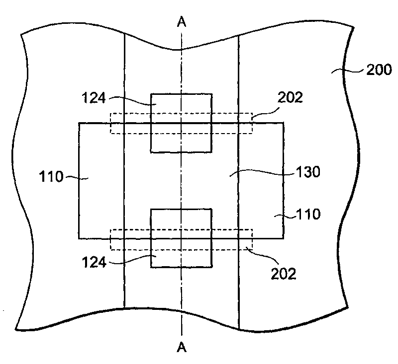
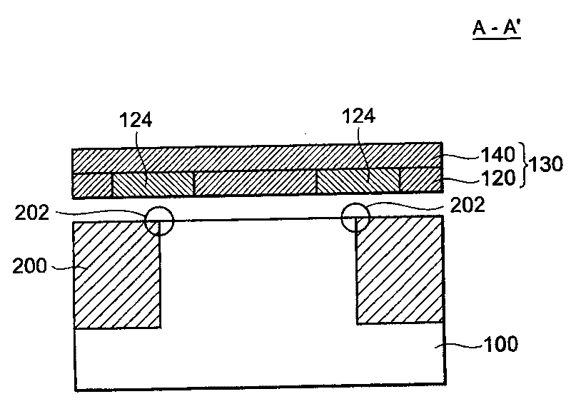
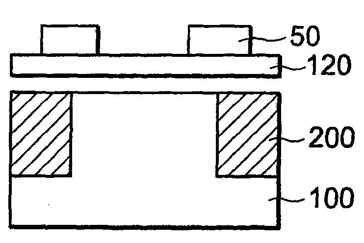
[0019] figure 1 A schematic plan view showing the structure of the semiconductor device according to the present embodiment. figure 1 The semiconductor device shown in includes an element isolation film 200, a gate electrode 130, and two impurity regions 110 which are a source region and a drain region. The element isolation film 200 is formed in the semiconductor layer and defines an element formation region. The gate electrode 130 is formed over the element formation region. Each end of the gate electrode 130 extends over the element isolation film 200 . Impurity region 110 is formed in the element formation region so as to sandwich the channel formation region below gate electrode 130 therebetween.

[0020] Two...


PUM


Abstract

Provided is a semiconductor device in which occurrence of humps can be suppressed and variations in characteristics of the semiconductor device can be suppressed. The semiconductor device includes: an element isolation film (200) formed in a semiconductor layer, the element isolation film (200) defining an element formation region; a gate electrode (130) formed above the element formation region, the gate electrode (130) having ends respectively extending above the element isolation film (200); and impurity regions (110) which are to be a source region and a drain region which are formed in the element formation region so as to sandwich therebetween a channel formation region immediately under the gate electrode (130), the gate electrode (130) including at each of the ends thereof a high work function region (124) in which work function is higher than work function in other regions over at least a part of an interface between the element formation region and the element isolation film (200).

Description

technical field [0001] The present invention relates to a semiconductor device in which peaks are suppressed. Background technique [0002] In recent years, higher integration of transistors has been required in response to demands for chip size reduction. One solution to this problem is an element isolation technique known as Shallow Trench Isolation (STI). However, when STI is employed, the gate oxide film becomes thinner at the interface between the diffusion layer portion and the STI portion than other portions, and thus, a parasitic transistor is formed. [0003] Figure 4 is a graph showing the relationship between gate voltage and drain current in a transistor having a parasitic transistor formed therein. exist Figure 4 In , curve A shows the relationship between the gate voltage and drain current in the main transistor, and curve B shows the relationship between the gate voltage and drain current in the parasitic capacitor. Equivalently, a transistor with a paras...

Claims


Application Information

Patent Timeline
Patent Type & Authority Applications(China)
IPC IPC(8): H01L27/088H01L29/78H01L29/06H01L29/423
CPCH01L29/78H01L29/4238
Inventor 田中浩治
Owner NEC ELECTRONICS CORP
Why Eureka
Try Eureka