

Semiconductor device and process of production of same
a technology of semiconductors and semiconductor substrates, applied in the direction of semiconductor devices, electrical devices, transistors, etc., can solve the problems of reducing the characteristics of transistors, difficult to completely remove the resist residue strongly adhesion to the semiconductor substrate or thermal oxide film and cvd insulating film, and unstable surface conditions, so as to prevent autodoping and prevent damage to elements
- Summary
- Abstract
- Description
- Claims
- Application Information
AI Technical Summary
Benefits of technology
Problems solved by technology
Method used
Image

Examples
first embodiment
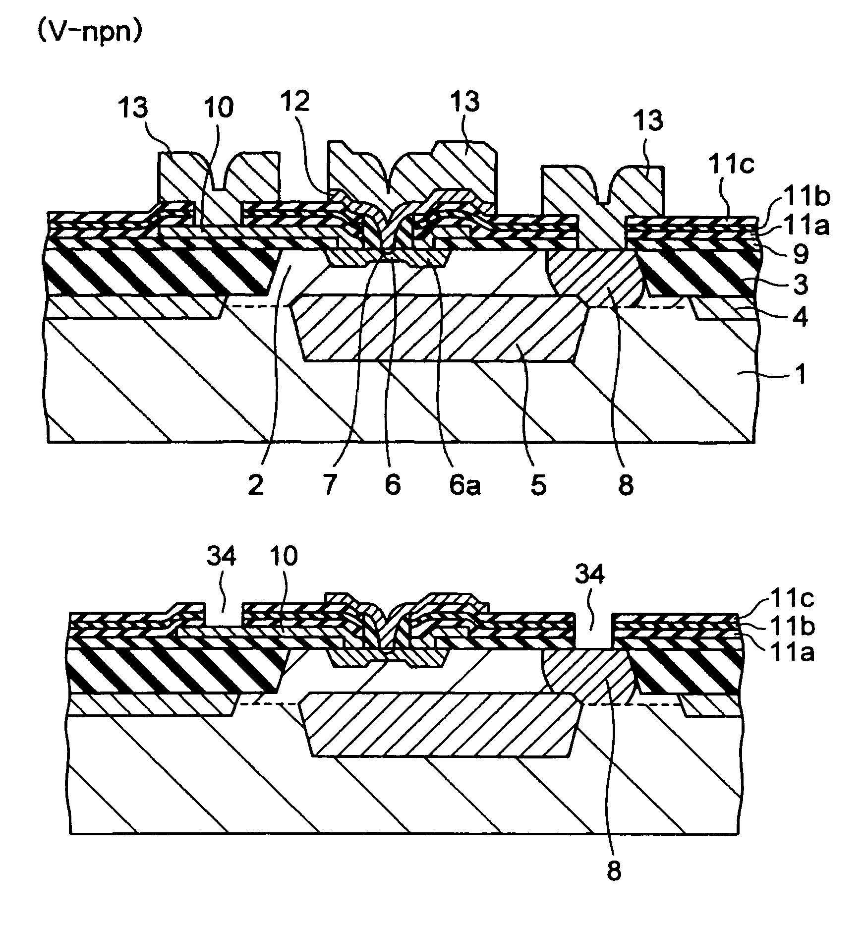
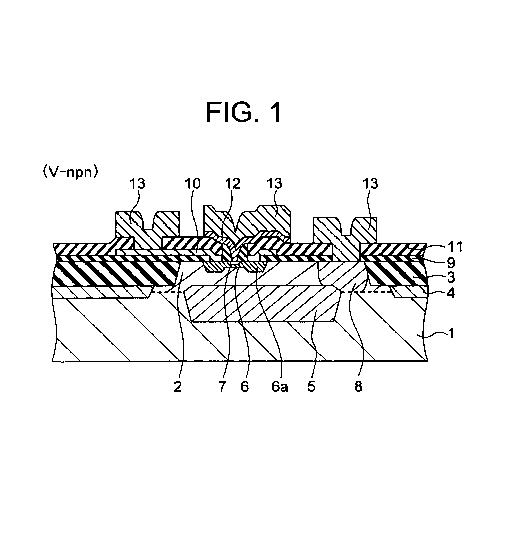
[0083](First Embodiment)
[0084]FIG. 5A is a cross-sectional view of a semiconductor device of the present embodiment and shows a vertical npn transistor (V-npn). As shown in FIG. 5A, on a p-type semiconductor substrate 1 is formed an n-type epitaxial layer 2. On the surface of the n-type epitaxial layer 2 is formed a LOCOS 3 for separating elements. Below the LOCOS 3 is formed an element separating diffusion layer 4 containing a p-type impurity. The element separating diffusion layer 4 reaches the p-type semiconductor substrate 1.
[0085]At the surface layer of the p-type semiconductor substrate 1 is formed an n-type collector buried layer 5 on which the n-type epitaxial layer 2 becomes an n-type collector layer. At the surface layer of the n-type epitaxial layer 2 comprised of the n-type collector layer is formed a p-type base region 6. Around the p-type base region 6 is formed a graft base 6a. At the surface layer of the p-type base region 6 is formed an n-type emitter region 7. Also...
second embodiment
[0110](Second Embodiment)
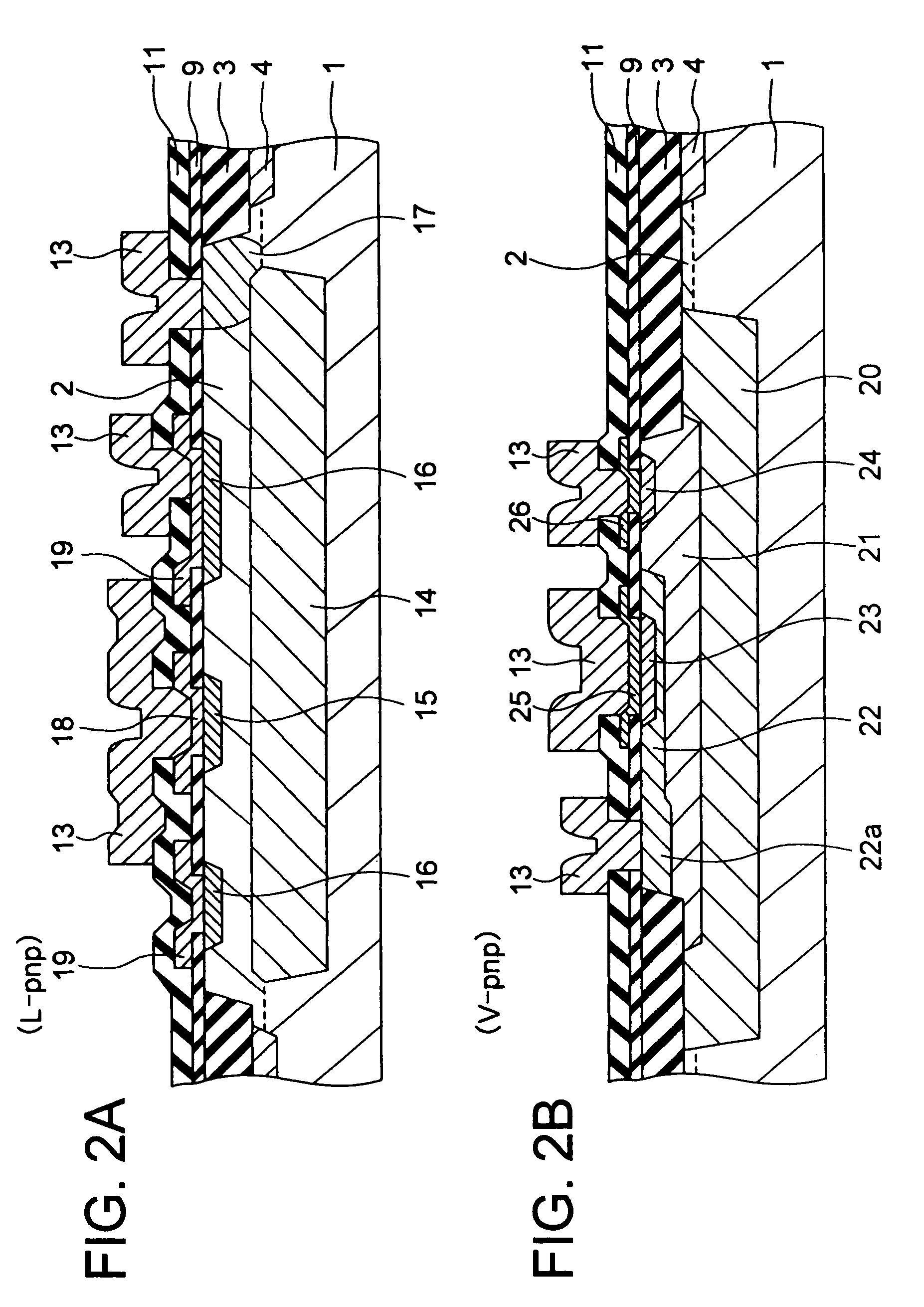
[0111]FIG. 11A is a cross-sectional view of a semiconductor device of the present embodiment and shows a lateral pnp transistor (L-pnp). As shown in FIG. 11A, on a p-type semiconductor substrate 1 is formed an n-type epitaxial layer 2. On the surface of the n-type epitaxial layer 2 is formed a LOCOS 3 for separating elements. Below the LOCOS 3 is formed an element separating diffusion layer 4 containing a p-type impurity. The element separating diffusion layer 4 reaches the p-type semiconductor substrate 1.
[0112]At the surface layer of the p-type semiconductor substrate 1 is formed an n-type base buried layer 14 whereon the n-type epitaxial layer 2 becomes an n-type base layer. At the surface layer of the n-type epitaxial layer 2 comprised of the n-type base layer are formed a p-type emitter region 15 and a p-type collector region 16 separate from each other. Also, in the n-type epitaxial layer 2 is formed a base plug region (n+ sinker) 17 connected to the n...
third embodiment
[0129](Third Embodiment)
[0130]FIG. 14A is a cross-sectional view of a semiconductor device of the present embodiment and shows a vertical pnp transistor (V-pnp). As shown in FIG. 14A, on a p-type semiconductor substrate 1 is formed an n-type epitaxial layer 2. On the surface of the n-type epitaxial layer 2 is formed a LOCOS 3 for separating elements. Below the LOCOS 3 is formed an element separating diffusion layer 4 containing a p-type impurity. The element separating diffusion layer 4 reaches the p-type semiconductor substrate 1.
[0131]At the surface layer of the p-type semiconductor substrate 1 is formed an n-type buried layer 20 whereon a p-well which becomes a p-type collector region 21 is formed. Due to the n-type buried layer 20, the p-type collector region 21 and p-type semiconductor substrate 1 are electrically separated. At the surface layer of the p-type collector region 21 formed an n-type base region 22 and graft base 22a connected to the base region 22. At the surface l...
PUM
 Abstract
Description
Claims
Application Information