Pixel electrode structure and liquid crystal display panel

一种液晶显示面板、像素电极的技术,应用在非线性光学、仪器、光学等方向,能够解决液晶有效电位降低、面板开口率降低、显示亮度下降等问题,达到优化电场分布、指向优化的效果

Active Publication Date: 2015-12-09
TCL CHINA STAR OPTOELECTRONICS TECH CO LTD
View PDF8 Cites 18 Cited by
  • Summary
  • Abstract
  • Description
  • Claims
  • Application Information

AI Technical Summary

Problems solved by technology

[0006] The conventional LCS structure improves the problem of color distortion in the large viewing angle display of the liquid crystal display panel
However, since the pixel electrodes of this type of liquid crystal display panel are divided into two display areas, this will inevitably lead to a reduction in the panel aperture ratio.
Moreover, for this type of liquid crystal display panel, the effective potential of the liquid crystal in the auxiliary display area will decrease, resulting in a decrease in the display brightness of this area, thereby affecting the transmittance of the panel.

Method used


Image

  • Pixel electrode structure and liquid crystal display panel
  • Pixel electrode structure and liquid crystal display panel
  • Pixel electrode structure and liquid crystal display panel

Examples


Embodiment 1

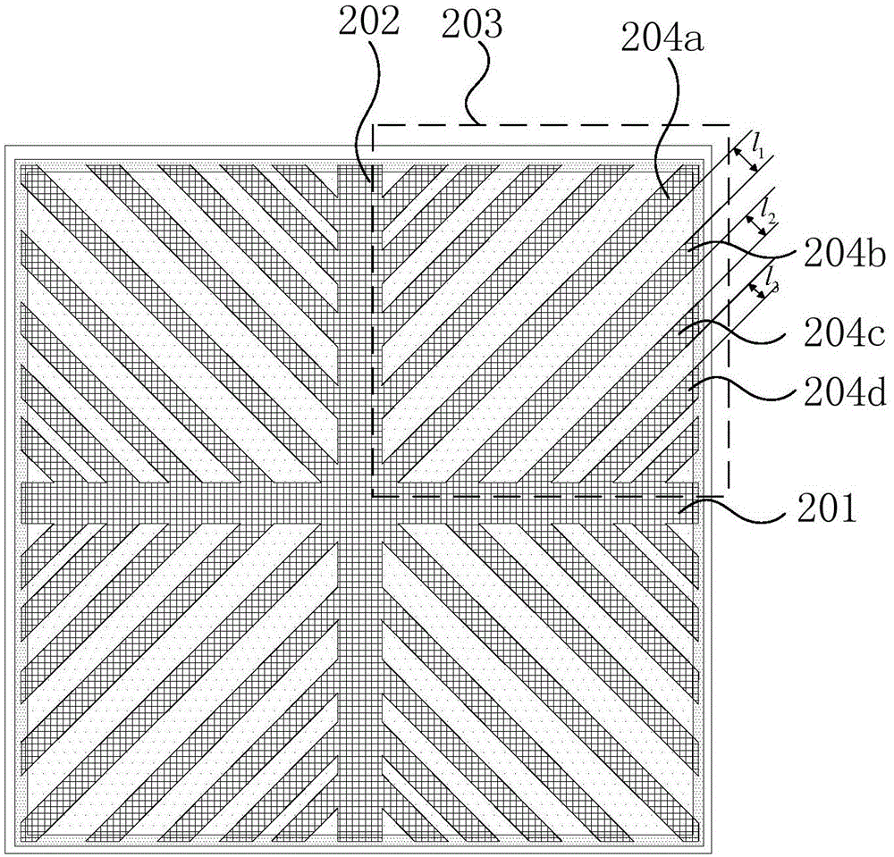
[0034] figure 2 A schematic diagram of the pixel electrode structure provided by this embodiment is shown.

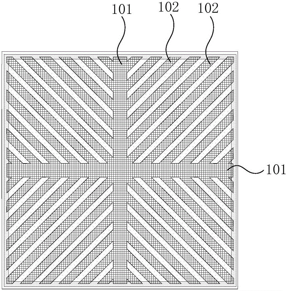
[0035] The pixel electrode structure provided in this embodiment includes: a first trunk electrode 201 , a second trunk electrode 202 and a plurality of branch electrodes. The first stem electrode 201 and the second stem electrode 202 perpendicularly intersect. In this way, in the pixel electrode structure, four liquid crystal alignment regions with different alignment directions are defined according to the extension directions of the branch electrodes. Wherein, the branch electrodes distributed in the same liquid crystal alignment region are parallel to each other, so that the distance between two adjacent branch electrodes is a certain value. The intersection point of the first stem electrode 201 and the second stem electrode 202 is the intersection point of the stem electrodes.

[0036] In this embodiment, the arrangement of each branch electrode in the four liq...

Embodiment 2

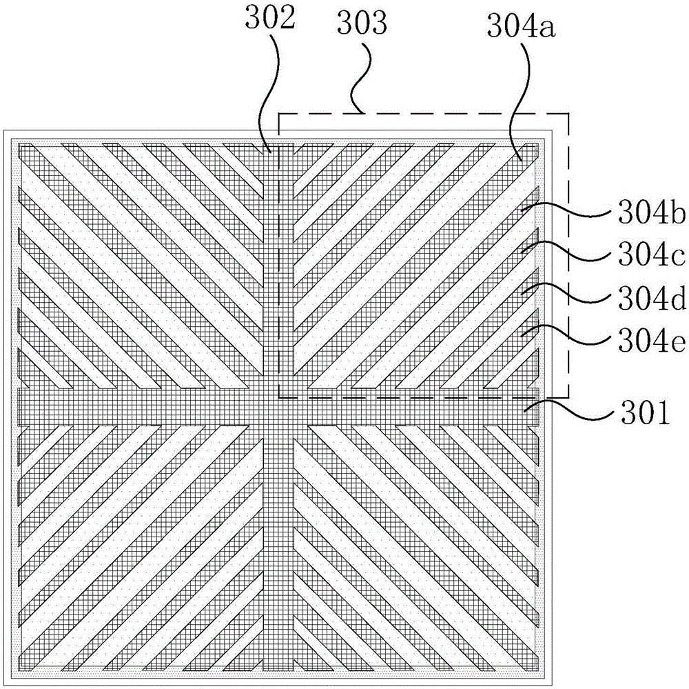
[0045] image 3 A schematic diagram of the pixel electrode structure provided by this embodiment is shown.

[0046] and figure 2 The electrode structure shown is similar, and the pixel electrode structure provided in this embodiment also includes: a first trunk electrode 301 , a second trunk electrode 302 and a plurality of branch electrodes. Wherein, the first trunk electrode 301 and the second trunk electrode 302 vertically intersect each other, thereby forming four liquid crystal alignment regions. The branch electrodes distributed in the same liquid crystal alignment area are parallel to each other. The intersection point of the first stem electrode 301 and the second stem electrode 302 is the intersection point of the stem electrodes.

[0047] In this embodiment, the arrangement of each branch electrode in the four liquid crystal alignment regions is symmetrical with respect to the first trunk electrode 301 and the second trunk electrode 302 . Therefore, for purposes...


PUM


Abstract

The invention discloses a pixel electrode structure and a liquid crystal display panel. The pixel electrode structure comprises a first main electrode, a second main electrode and a plurality of branch electrodes, wherein the first main electrode and the second main electrode are intersected and form multiple liquid crystal distribution areas; one end of each branch electrode is at least connected with one of the first main electrode and the second main electrode, and the branch electrodes distributed in the same liquid crystal distribution area are parallel to each other; in the same liquid crystal distribution area, the intervals between the adjacent branch electrodes are reduced gradually along the direction far away from the central area of the liquid crystal distribution area. According to the pixel electrode, the distribution of the electric fields of the electrodes is optimized, and further the direction of the liquid crystal is optimized, so that the large-viewing-angle of the liquid crystal panel can be improved on the basis of guaranteeing the aperture opening ratio.

Description

technical field [0001] The invention relates to the technical field of liquid crystal display, in particular to a pixel electrode structure and a liquid crystal display panel. Background technique [0002] With the development of thin film transistor liquid crystal displays and the progress of industrial technology, the manufacturing process of liquid crystal displays is becoming more and more perfect, and the manufacturing cost of liquid crystal displays is also getting lower and lower. Liquid crystal displays have replaced cathode ray tube displays as the mainstream display in the field of everyday display. [0003] As a branch of the VA liquid crystal display panel, the HVA liquid crystal display panel adopts the method of photo-alignment and electrification to solidify a liquid crystal layer with a certain pre-tilt angle on the surface of the guide film, so as to omit the traditional rubbing alignment process. [0004] figure 1 A schematic structural diagram of a pixel...

Claims


Application Information

Patent Timeline
Patent Type & Authority Applications(China)
IPC IPC(8): G02F1/1343G02F1/1337
CPCG02F1/133707G02F1/134309G02F1/133742G02F1/133753G02F2201/122G02F2201/123G02F1/133757
Inventor 姚晓慧许哲豪
Owner TCL CHINA STAR OPTOELECTRONICS TECH CO LTD
Why Eureka
Try Eureka