Power semiconductor device and manufacturing technology

A technology for power semiconductors and manufacturing processes, which is applied in the field of trench-type power semiconductor devices and manufacturing processes, and can solve the problems of low electric field, excessive electric field, vertical electric field distribution and trapezoidal distribution of silicon and silicon dioxide, etc. , to achieve the effects of increased epitaxial concentration, improved electric field distribution, and reduced depleted epitaxial thickness

Active Publication Date: 2014-12-24
CHINA RESOURCES MICROELECTRONICS (CHONGQING) CO LTD
View PDF4 Cites 11 Cited by
  • Summary
  • Abstract
  • Description
  • Claims
  • Application Information

AI Technical Summary

Problems solved by technology

[0003] The vertical electric field of the conventional Split-gate MOSFET structure is a bimodal distribution, although it is better than the triangular distribution of the ordinary Trench MOS, but no matter how to optimize the epitaxial concentration and Trench spacing, its vertical electric field distribution is difficult to achieve the trapezoidal distribution of the superjunction
The reason is that the potential at the bottom of the trench is the largest, and the curvature effect causes the electric field to be too large. In addition, the silicon potential at the middle of the trench is low, which leads to the low electric field of silicon and silicon dioxide there.

Method used


Image

  • Power semiconductor device and manufacturing technology
  • Power semiconductor device and manufacturing technology
  • Power semiconductor device and manufacturing technology

Examples


Embodiment Construction

[0053] In the following description, numerous specific details are given in order to provide a more thorough understanding of the present invention. It will be apparent, however, to one skilled in the art that the present invention may be practiced without one or more of these details. In other examples, some technical features known in the art are not described in order to avoid confusion with the present invention.

[0054] In order to thoroughly understand the present invention, detailed steps and detailed structures will be provided in the following description, so as to illustrate the technical solution of the present invention. Preferred embodiments of the present invention are described in detail below, however, the present invention may have other embodiments besides these detailed descriptions.

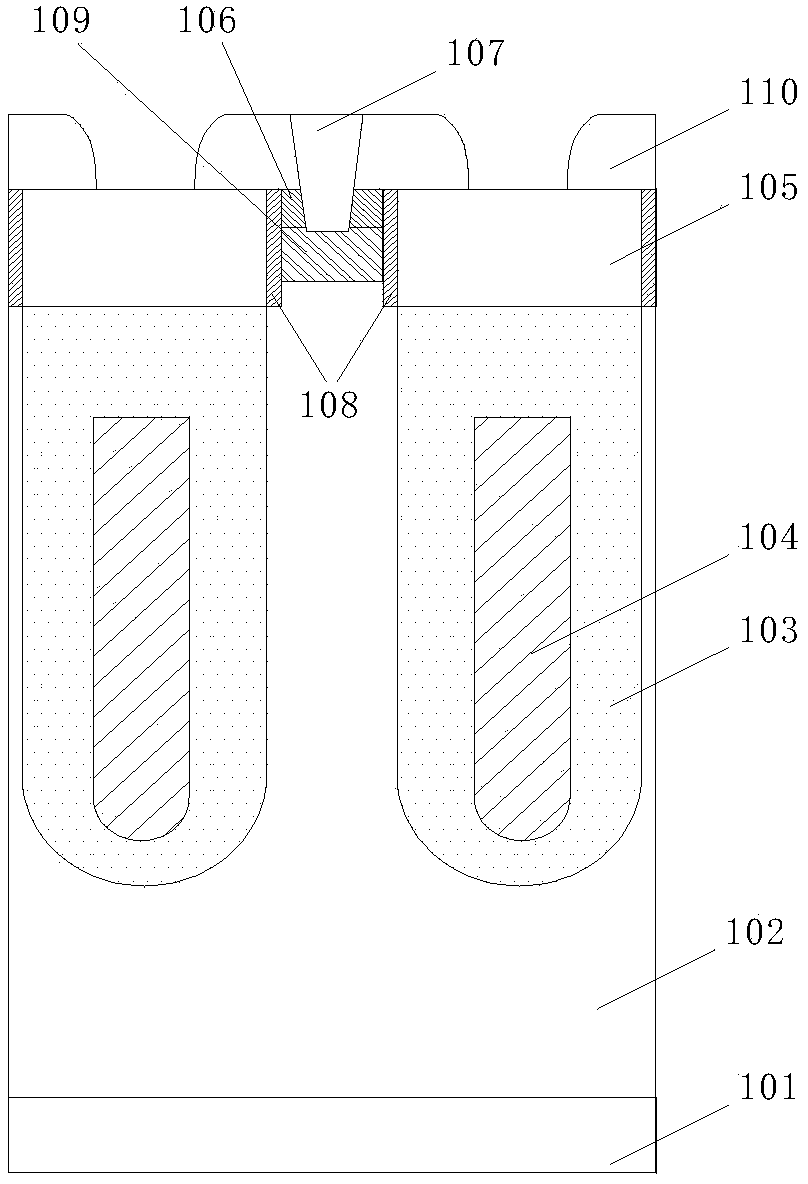
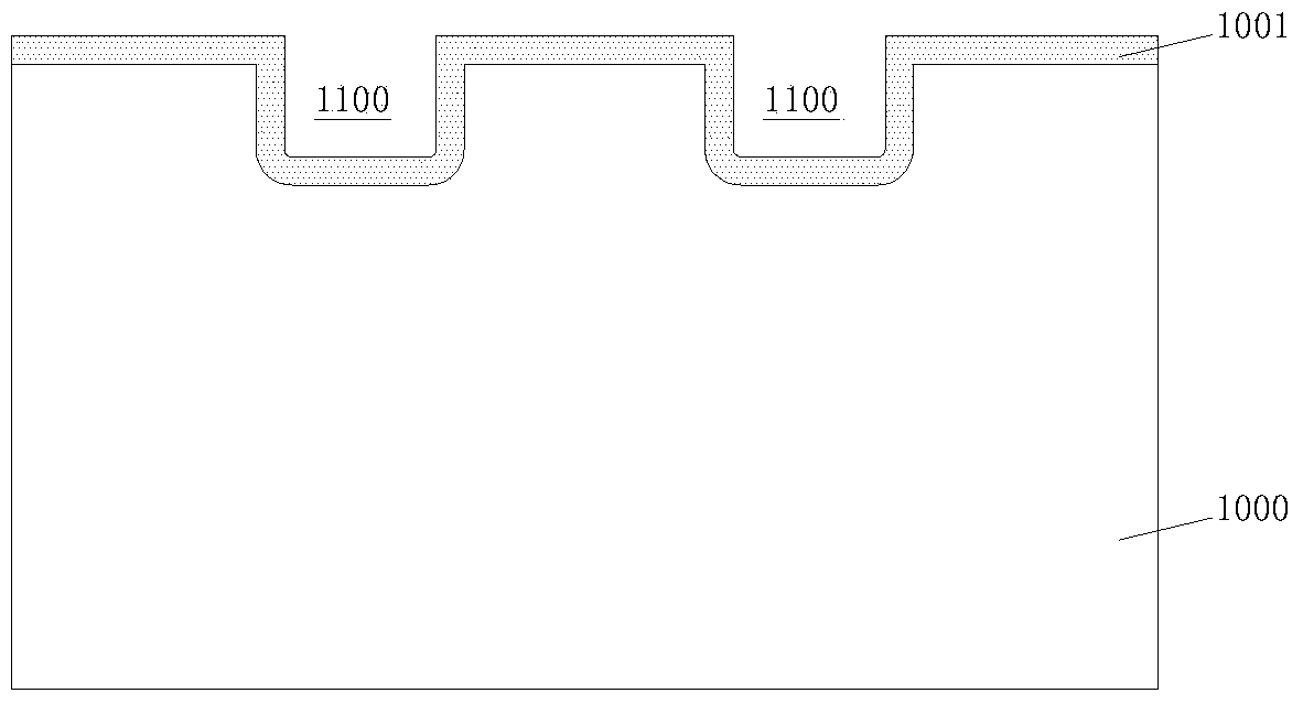
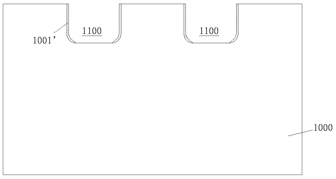
[0055] The purpose of the present invention is to provide a high-density RESURF (surface electric field modulation) oxide layer, and a MOS device with a similar inclined sid...


PUM


Abstract

The invention provides a power semiconductor device and a manufacturing method. A RESURF oxide layer with the thickness gradually reduced in a step mode from bottom to top is manufactured on the side wall of a groove, the distance between gate oxides is enlarged, and therefore under the premise of the same cell pitch width and the same trench width, the epitaxy concentration is doubled, the conduction resistance is effectively reduced, and the epitaxy thickness is effectively exhausted during breakdown. The structure conforms to a reasonable design rule, and the optimization of the conduction resistance is achieved simply with the simple resurf structure.

Description

technical field [0001] The present invention relates to the field of semiconductors, specifically, to a trench-type power semiconductor device and a manufacturing process. Background technique [0002] In the field of power electronics, a power MOSFET (Metal-Oxide-Semiconductor Field Effect Transistor, Metal-Oxide-Semiconductor Field Effect Transistor) is widely used in a switching device structure. In order to make the function of the switching device play well, the power MOSFET needs to meet two requirements: 1. When the device is in the on state, it can have a very low on-resistance to minimize the power loss of the device itself; 2. When the device is in the In the off state, it can have a sufficiently high reverse breakdown voltage. Super Junction is called a milestone invention of power devices, which greatly improves the epitaxial concentration of power devices under the same withstand voltage and reduces the specific on-resistance of devices. A new type of trench M...

Claims


Application Information

Patent Timeline
Patent Type & Authority Applications(China)
IPC IPC(8): H01L29/78H01L29/06H01L21/336
CPCH01L29/4236H01L29/66446H01L29/66666
Inventor 赖海波
Owner CHINA RESOURCES MICROELECTRONICS (CHONGQING) CO LTD
Why Eureka
Try Eureka