

SOI-LIGBT device capable of suppressing Snapback phenomenon and manufacturing method thereof
A technology of devices and phenomena, applied in the field of SOI-LIGBT devices and their manufacturing, can solve problems affecting device performance and achieve the effects of reducing device area, reducing device cost, and uniform distribution
- Summary
- Abstract
- Description
- Claims
- Application Information
AI Technical Summary
Problems solved by technology
Method used
Image

Examples
Embodiment 1
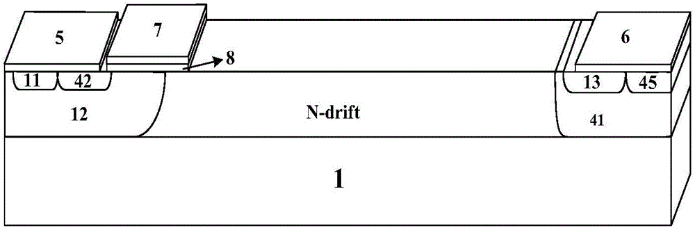
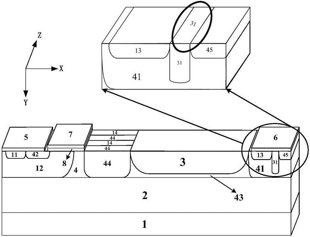
[0058] Such as figure 2 as shown, figure 2 It is a schematic diagram of an SOI-LIGBT device capable of suppressing the Snapback phenomenon in this embodiment; its cell structure includes a substrate 1, a buried oxide layer 2 on the upper surface of the substrate 1, a thick dielectric layer 3 above the buried oxide layer 2, a thick The thick silicon layer drift region 4 on the left side of the dielectric layer 3, the P well region 12 at the left end inside the thick silicon layer drift region 4, the mutually independent P-type heavily doped emitter region 11 and the first P well region 12 arranged inside the P well region An N-type heavily doped region 42, an N-type buffer region 41 disposed at the right end of the thick dielectric layer 3 along the longitudinal direction, a P-type heavily doped collector region 13 at the left end inside the N-type buffer region 41, and an N-type buffer region 41 The second N-type heavily doped region 45 at the inner right end, the collector...
Embodiment 2
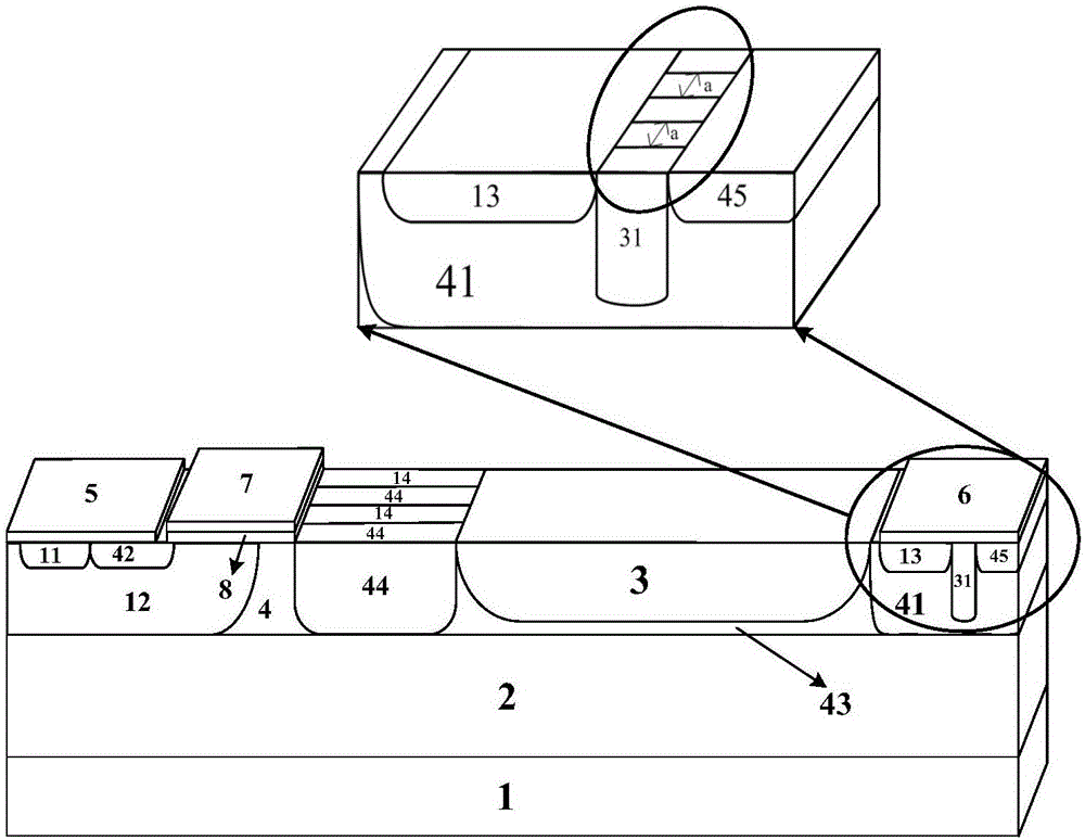
[0075] Such as image 3 As shown, this embodiment is basically the same as Embodiment 1, the difference is that: the collector dielectric barrier layer 31 in this embodiment includes a plurality of sub-barrier layers separated by N-type buffer regions 41 in the Z direction, adjacent sub-barrier layers The distance between the barrier layers in the Z direction is a.
Embodiment 3
[0077] Such as Figure 4 As shown, this embodiment is basically the same as Embodiment 1, with the difference that: in this embodiment, the N strips 44 and the P strips 14 are not in contact with the upper surface of the buried oxide layer 2 .
PUM
 Abstract
Description
Claims
Application Information