SOI (Silicon On Insulator) type P-LDMOS (Lateral Diffused Metal-Oxide Semiconductor)

A P-LDMOS, semiconductor technology, applied in electrical components, circuits, semiconductor devices, etc., can solve the problems of limiting the vertical breakdown voltage of SOI type P-LDMOS, difficulty in forming dielectric isolation regions, and difficulty in process implementation, etc. High-voltage application range, the effect of increasing the longitudinal breakdown voltage, and improving the withstand voltage capability

Inactive Publication Date: 2013-10-02
UNIV OF ELECTRONICS SCI & TECH OF CHINA
View PDF1 Cites 0 Cited by
  • Summary
  • Abstract
  • Description
  • Claims
  • Application Information

AI Technical Summary

Problems solved by technology

However, if the S layer is too thick, it will be difficult to form a dielectric isolation region in the S layer; if the I layer is too thick, it will be difficult to implement the process, and it is not conducive to heat dissipation of the device.
Therefore, limited by the device structure and process, both the S layer and the I layer cannot be too thick, which limits the improvement of the vertical breakdown voltage of SOI type P-LDMOS, which in turn limits the improvement of its breakdown voltage and affects its application range.

Method used


Image

  • SOI (Silicon On Insulator) type P-LDMOS (Lateral Diffused Metal-Oxide Semiconductor)
  • SOI (Silicon On Insulator) type P-LDMOS (Lateral Diffused Metal-Oxide Semiconductor)
  • SOI (Silicon On Insulator) type P-LDMOS (Lateral Diffused Metal-Oxide Semiconductor)

Examples


Embodiment 1

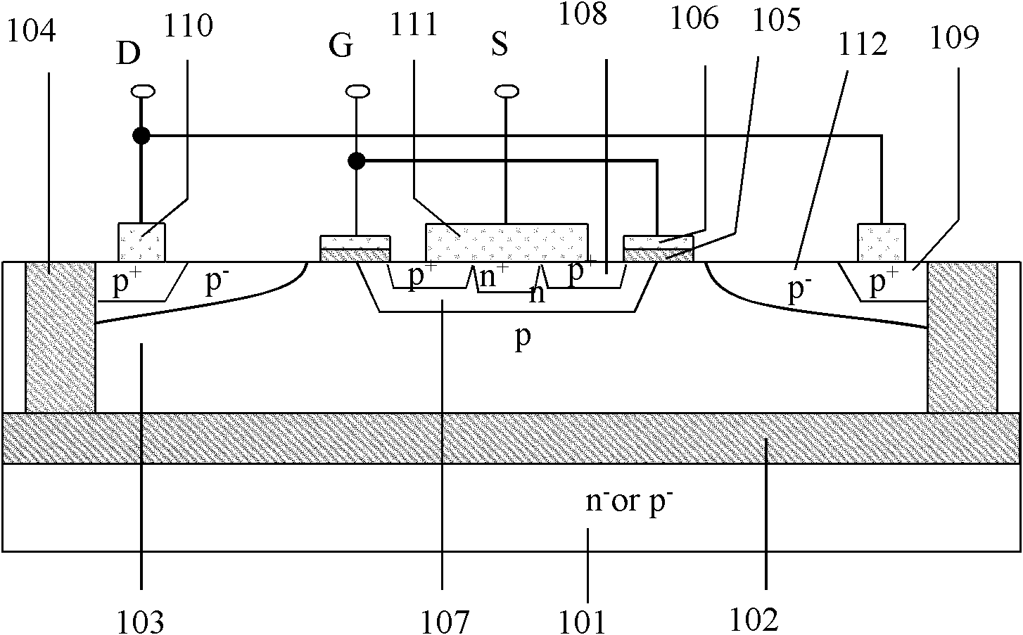
[0069] This embodiment provides an SOI type P-LDMOS, such as Figure 4 As shown, it is a schematic diagram of a local structure of the device, including: a semiconductor substrate layer 101, a dielectric buried layer 102, a semiconductor active layer 103, and a dielectric isolation region 104. The two dielectric isolation regions define the active region of the device. A gate oxide layer 105, a gate electrode 106 on the gate oxide layer 105, an n well 107 in the active region, a p well in the n well 107 + source region 108, p + The drain region 109 is formed on the drain region and the drain electrode 110 is formed on the p + The source electrode 111 on the source region 108 .

[0070] The semiconductor active layer 103 has a plurality of n + The doped region 113 is located on the semiconductor active layer 103 side of the interface between the dielectric buried layer 102 and the semiconductor active layer 103 .

[0071] At the same time, one difference between the P-LDMOS...

Embodiment 2

[0082] In order to solve the self-heating effect of SOI type P-LDMOS, this embodiment provides another structure of SOI type P-LDMOS, such as Figure 9 Shown is a schematic diagram of the local structure of the device.

[0083] The SOI type P-LDMOS includes: a semiconductor substrate layer 101, a dielectric buried layer 102, a semiconductor active layer 103 and n + Doped region 113, n + The doped region 113 is located on the semiconductor active layer 103 side of the interface between the buried dielectric layer 102 and the semiconductor active layer 103 , and a silicon window 114 for heat dissipation may also be provided in the buried dielectric layer 102 .

[0084] Specifically, one or more silicon windows 114 may be provided in the dielectric buried layer 102, and the distribution range of each silicon window may be equal or different.

[0085] This embodiment focuses on the differences from the SOI-type P-LDMOS provided in Embodiment 1, and the similarities can be referr...

Embodiment 3

[0087] Such as Figure 10 Shown is a schematic diagram of a partial structure of the SOI type P-LDMOS provided in this embodiment.

[0088] The SOI type P-LDMOS includes: a semiconductor substrate layer 101, a dielectric buried layer 102, a semiconductor active layer 103 and an n+ doped region 113, and the n+ doped region 113 is located at the interface between the dielectric buried layer 102 and the semiconductor active layer 103 one side of the semiconductor active layer 103;

[0089] the n + A dielectric groove 115 is arranged in the space between the doped regions 113, and the material of the dielectric groove 115 is SiO 2 , Low dielectric constant material or variable dielectric constant material.

[0090] Such as Figure 11 As shown in , it is a schematic diagram of another partial structure of the SOI type P-LDMOS provided in this embodiment.

[0091] The SOI type P-LDMOS includes: a semiconductor substrate layer 101, a dielectric buried layer 102, a semiconductor ...


PUM


Abstract

An SOI type P-LDMOS is provided, comprising: a semiconductor substrate layer (10), a dielectric buried layer (102) and a semiconductor active layer (103). There are multiple spaced n+ doped regions (113) in the semiconductor active layer, placed on the interface between the dielectric buried layer and the semiconductor active layer, and on the side of the semiconductor active layer. And, there are no light-doped drain regions in the semiconductor active layer.

Description

Technical field: [0001] The invention relates to the technical field of semiconductor power devices, in particular to an SOI type P-LDMOS. Background technique: [0002] SOI (Semiconductor On Insulator, silicon on insulating substrate) power devices have the advantages of high operating speed and integration, good insulation performance, strong radiation resistance, and no thyristor self-locking effect, so , the application of SOI power devices in the field of VLSI has been widely concerned, but it has defects such as low breakdown voltage and self-heating effect, which limit its application range. The breakdown voltage of an SOI power device depends on the lower of the lateral breakdown voltage and the vertical breakdown voltage. In the control of lateral breakdown voltage, the existing mature Si-based device lateral withstand voltage design principles and technologies can be used. Therefore, how to improve the vertical breakdown voltage has become a difficult point in the...

Claims


Application Information

Patent Timeline
Patent Type & Authority Patents(China)
IPC IPC(8): H01L29/78H01L29/06
CPCH01L29/0623H01L29/7824H01L29/78603
Inventor 张波吴丽娟乔明胡盛东胡曦李肇基
Owner UNIV OF ELECTRONICS SCI & TECH OF CHINA
Why Eureka
Try Eureka