Silicon-on-insulator LDMOS (Laterally Diffused Metal Oxide Semiconductor) transistor with multiple triangular buried layers

A silicon-on-insulating layer, triangular technology, applied in the direction of semiconductor devices, electrical components, circuits, etc., to achieve the effect of improving breakdown voltage, increasing current, and uniform distribution of lateral electric field

Pending Publication Date: 2022-05-27
杭州电子科技大学温州研究院有限公司 +1
View PDF0 Cites 0 Cited by
  • Summary
  • Abstract
  • Description
  • Claims
  • Application Information

AI Technical Summary

Problems solved by technology

However, the structure of the existing silicon LDMOS transistor on the insulating layer still has room for further improvement, and its breakdown voltage and on-resistance performance need to be further improved.

Method used


Image

  • Silicon-on-insulator LDMOS (Laterally Diffused Metal Oxide Semiconductor) transistor with multiple triangular buried layers
  • Silicon-on-insulator LDMOS (Laterally Diffused Metal Oxide Semiconductor) transistor with multiple triangular buried layers
  • Silicon-on-insulator LDMOS (Laterally Diffused Metal Oxide Semiconductor) transistor with multiple triangular buried layers

Examples


Embodiment 1

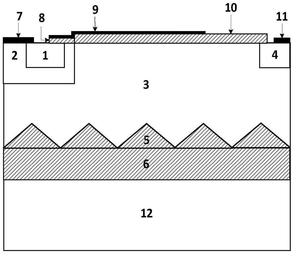
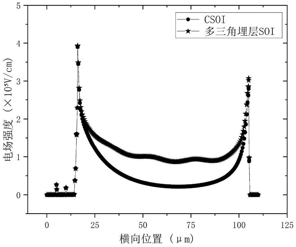
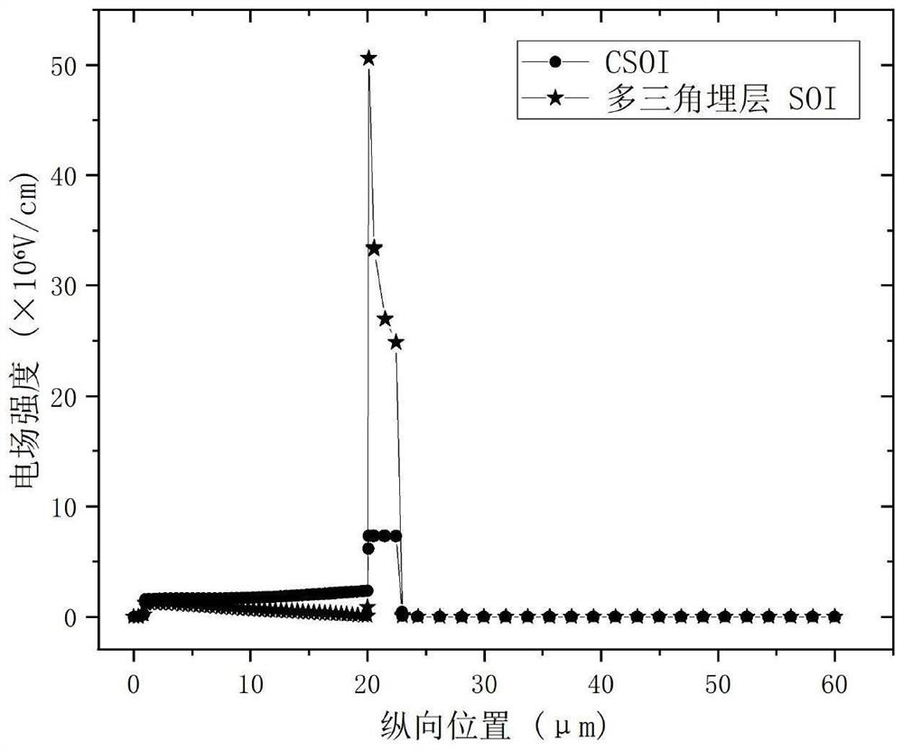
[0024] Based on the above parameters, the thickness of the source region 1 and the drain region 4 are both 1 μm; the thickness of the silicon body 2 is 8 μm; the thickness of a single triangular buried oxide layer 5 is 10 μm, the bottom length is 22 μm, and the number is 5 ; The length of the fully buried oxide layer 6 is 110 μm; the doping concentration of the drift region is 4×10 14 cm -3 ; The simulation simulation obtains the silicon-on-silicon LDMOS transistor (referred to as MTBL SOI LDMOS, abbreviated as MTBL SOI) of the present invention with a plurality of triangular buried layers on the silicon film layer. The surface electric field varies with the lateral position curve, and is better than the traditional The performance of the silicon-on-insulator LDMOS transistor (referred to as CSOI LDMOS, abbreviated as CSOI) of the surface electric field on the silicon film layer with the lateral position curve is compared, such as figure 2 As shown, it can be seen that the i...

Embodiment 2

[0029] Change the height h (or thickness, i.e. the vertical distance from the vertex to the bottom of the triangular buried oxide layer) of the triangular buried oxide layer, and the remaining parameters are the same as those of Example 1;

[0030] like Image 6 As shown, as the height h of the multiple triangular buried oxide layers increases, the breakdown voltage of the device of the present invention first increases and then decreases. The optimum height of the triangular buried oxide layer is 10 μm, that is, h=10 μm.

Embodiment 3

[0032] Change the width d (or length, that is, the length of the bottom side of the triangular buried oxide layer) of the multiple triangular buried oxide layers, and the doping concentration of the drift region, and the remaining parameters are the same as those in Example 1;

[0033] like Figure 7 As shown, when the width d of the triangular buried oxide layer is constant, with the increase of the doping concentration of the drift region, the breakdown voltage of the device of the present invention first increases and then decreases; With the increase of d, the peak value of the breakdown voltage corresponding to each d decreases with the variation of the doping concentration in the drift region, but the peak difference is not significant when d is 16 μm, 20 μm and 22 μm.

[0034] like Figure 8 As shown, when the width d of the triangular buried oxide layer remains unchanged, with the increase of the doping concentration of the drift region, the on-resistance of the devic...


PUM

PropertyMeasurementUnit
lengthaaaaaaaaaa
thicknessaaaaaaaaaa
thicknessaaaaaaaaaa

Abstract

The invention discloses a silicon-on-insulator LDMOS (Laterally Diffused Metal Oxide Semiconductor) transistor with a plurality of triangular buried layers. A fully buried oxide layer is arranged on a substrate layer; a silicon film layer is arranged on the fully buried oxide layer; the silicon film layer comprises a source region, a silicon body, a drift region, a drain region and a plurality of triangular buried oxide layers; the source region and the silicon body are located at one side of the silicon film layer, the silicon body surrounds the source region, and the source region is located at the top of the silicon film layer; the drain region is located at the top of the other side of the silicon film layer; a region among the drain region, the silicon body and the plurality of triangular buried oxide layers is a drift region; the plurality of triangular buried oxide layers are positioned above the fully buried oxide layer; the channel is provided by a silicon body between the source region and the drift region; the gate oxide layer is positioned above the channel and the drift region; the extended oxide layer is positioned above the drift region; two adjacent side surfaces of the extended oxide layer and the gate oxide layer are in contact; the gate oxide layer is completely covered by the gate electrode, and the extended oxide layer is partially covered by the gate electrode; the source electrode is located above the source region, and the drain electrode is located above the drain region. According to the invention, the breakdown voltage and the on-resistance performance are more excellent.

Description

technical field [0001] The invention belongs to the field of devices for semiconductor high-voltage power integrated circuits, and in particular relates to a silicon-on-insulator (Silicon-On-Insulator, SOI) substrate with multiple triangular buried oxide layers (Multiple Triangle Buried Oxide Layer, MTBOX) at the same time. The Lateral Double-diffused Metal-Oxide-Semiconductor (LDMOS) transistor is a silicon-on-insulator transistor (Multiple Triangle Buried Oxide Layers SOI LDMOS, MTBOX SOI LDMOS) with multiple triangular buried layers. Background technique [0002] With the development of semiconductor process technology and power integrated circuits, the demand for high-voltage and high-power semiconductor devices in the society is increasing day by day, and the society's performance requirements are getting higher and higher, so the improvement of the performance of high-voltage devices has become particularly important. The function of increasing the buried oxide layer i...

Claims


Application Information

Patent Timeline
Patent Type & Authority Applications(China)
IPC IPC(8): H01L29/06H01L29/78
CPCH01L29/7824H01L29/0684H01L29/0657H01L29/0611H01L29/0615
Inventor 胡月张慧丁怡王高峰
Owner 杭州电子科技大学温州研究院有限公司
Why Eureka
Try Eureka